This article describes the architecture, implementation and usage example of PWM module as a part of processor peripheral system.
Architecture overview
The Yet Another PWM is designed in modular manner - it can be reused in both systems with and without bus Master.
The PWM Core can be used when design have no bus Master - the Division Factor, Pulse and Period Length can be set
directly on the appropriate data lines by the Source. For example clock division factor and period lengths can be set as a
constant value while pulse lengths will be updated by UART data.
The PWM Module (incorporates PWM Core + bus interface) can be used in the systems with CPU/DMA or any other bus Master.
Block diagram:
Pulse Modulator
The heart of any PWM module is a counter clocked by an reference frequency, comparator
(two comparators in our case for flexible adjustment of period and pulse lengths) and output control logic
to generate pulse width modulated waveform. The pulse and period lengths values are stored
in two active registers. To maintain data reloading only after cycle completion (at the end of period)
another pair of shadow registers is used in conjunction with active registers (on the PWM Module level,
while active registers are part of PWM Core). Data from shadow registers reloads into active
registers only after Period Match signal is set or can be forced (during active period) by Pwm Reset strobe
pulse (asynchronous reset).
When counter matches the pulse length active register value - the output (JK flip-flop) is reset and after
it matches period length active register value - the output is set. At the end of each cycle (period length match) the
Period Match is set synchronously resetting counter and enabling reloading of new value from shadow registers into
active registers.
Clock divider
The integer clock divider is used to achieve higher flexibility of PWM Core.
It is formed by counter and comparator. The division factor value is set on
DivFactor bus. Divider Reset strobe pulse (asynchronous reset) should be set after applying new DivFactor value
to reset counter and apply it immediately. To bypass integer clock divider DivFactor should be set to 0.
The counter increments its value at each input clock cycle by 1. Comparator generates match signal when counter value matches
the value on DivFactor bus and synchronously resets counter. The match signal becomes divided clock and is used by
Pulse Modulator as clock enable signal, allowing design to be synchronous and run in one clock domain.
Detailed schematic:
Implementation
Pulse Width Modulator Core component
The Verilog source code of PWM Core can be found here: PWMCore.v
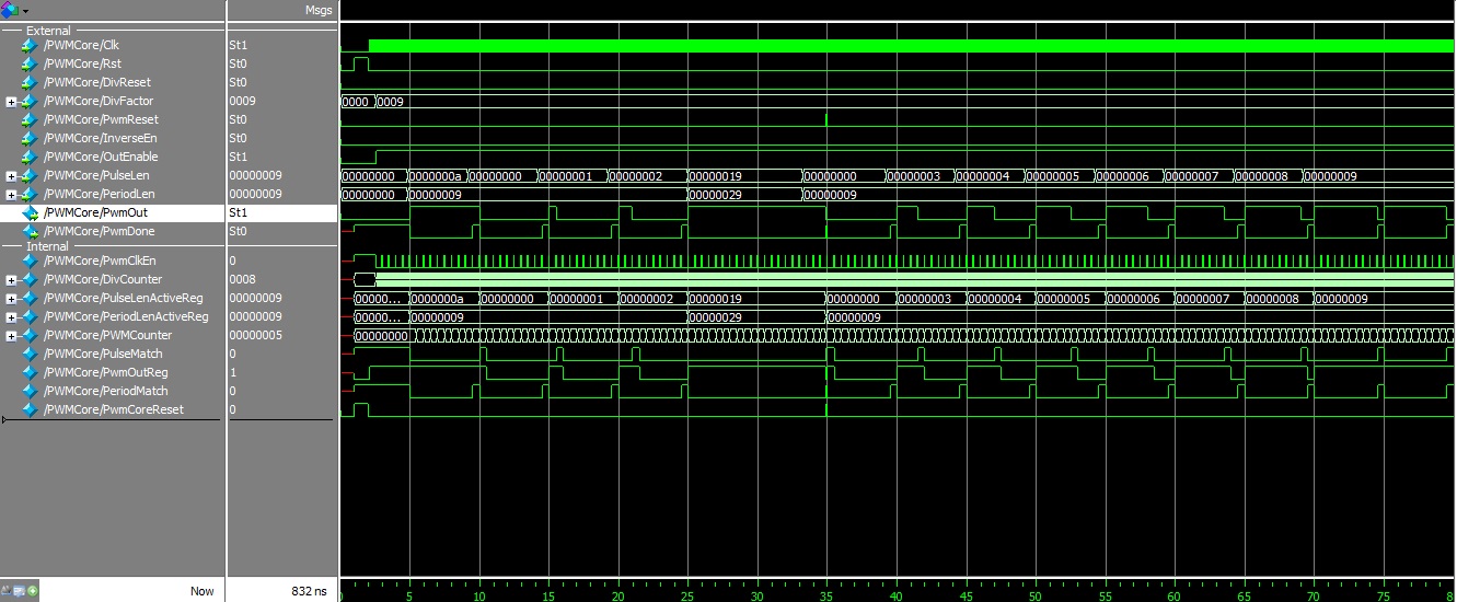
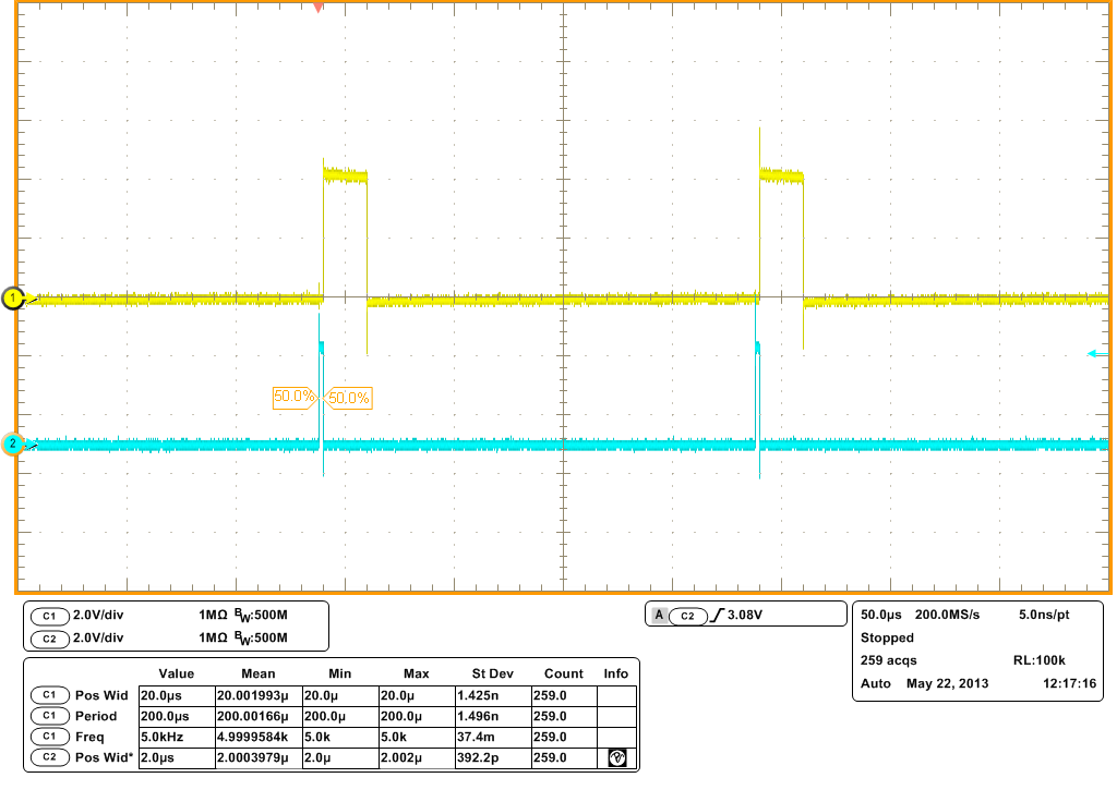
PWM Core simulation results:
Built into Nios II processor system
To embed any module into any microprocessor system the module control interface should be designed. Also address range
should be assigned to peripheral module registers.
In our case we are going to use Altera NiosII CPU and Avalon bus for PWM Module connection.
The bus conduit was added into NiosII processor system to export Avalon address, data buses and control signals.
Note: System clock (and PWM Module) frequency - 50MHz.
Usage example
An example application using 10 PWM units was designed. Sine wave was generated in the CPU and
displayed by 10 LEDs with phase shift.
Sine generator:
The NiosII CPU source code can be found at: main.c
Sine wave demo video:
The full QuartusII and NiosII EDS project utilizing
Altera DE0 Board
can be download here (~30MB): PWM_Project.zip
Note: NiosII BSP file link is static, to compile it the PWM_Project should be unzipped to D:/Study/
Future expansion
The good idea for future expansion might be:
1. Generate complementary output to drive push-pull circuits.
2. Add Dead Time generator for efficient push-pull transistor circuits driving.
3. Implement multiple phase PWM Module.
4. Add Phase Delay for multiple phase PWM flexibility.