


Introduction to FPGA Technology
Overview
FPGA stands for Field Programmable Gate Array. An FPGA is an integrated circuit (IC) that can be programmed and configured by the embedded system developer in the field after it has been manufactured. FPGA is a semi-conductor device which is not limited to any pre-defined hardware function; it is rather highly flexible in its functionality and may be configured by the embedded system developer according to his design requirements. FPGAs use pre-built logic blocks and programmable routing channels for implementing custom hardware functionality depending upon how embedded system developer configure these devices. The FPGAs are programmed and configured using hardware description languages (HDL) like Verilog and VHDL, similar to that used for an application-specific integrated circuit (ASIC).
FPGAs give a lot of flexibility to the embedded systems developer to program features and functions of their FPGA based product even after the FPGA based product has been installed in the field. This is the reason why FPGA is termed field programmable, as FPGA may easily be reconfigured and reprogrammed in the field according to new features and end-user’s requirements. FPGAs are being widely used in digital electronic circuits and embedded systems design and FPGAs have a well-defined place in every embedded system developer’s toolbox.
FPGAs may be used to implement any logical functions and features that an Application-Specific Integrated Circuit (ASIC) could possibly be utilized to implement. But in terms of flexibility of upgrading and modifying the functionality and features of FPGAs, even after the FPGA based product has been shipped to the end-user, FPGAs really have an edge over ASIC.
Internal Architecture of FPGA
There are several different families of FPGAs, manufactured by different semiconductor companies like Xilinx, Altera and Actel etc., that are currently available in market. These device families, when compared with one another, show slight variations in their features and architecture. Despite the slight differences in their architecture and features, on the whole, these device families follow a common design methodology. A brief description of internal architecture of FPGA is given below.
The FPGAs are composed of hundreds or thousands of logic cells. A “logic-cell” in turn is composed of three basic components: a small Lookup Table (LUT), a D-Flip-flop and a 2-to-1 Multiplexer.
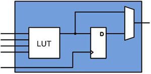
As shown in Figure 1, if required, the Multiplexer may be used to bypass the flip-flop. Flip-flops are binary shift registers, which are used to synchronize logic and save logical states between clock cycles. On every clock edge a flip-flop latches a 1 or 0 value on its input and holds that value constant until the next clock edge. A LUT may be regarded as a small RAM which is capable of implementing any logic function.
Each logic-cell when taken individually may of little use. However, a large number of logic-cells when connected together may be employed for implementation of complex logical functions. FPGAs are equipped with fairly a large number of routing resources (Multiplexers or wires placed around the logic cells) for connecting together a huge number of logic cells for implementation of complex and useful logical functions.
The IOBs (IO Blocks), which are implemented at the boundary of the FPGA chip, provide connection between internal logic and the package pins for interfacing the internal logic cells with the components connected externally with the FPGA chip.
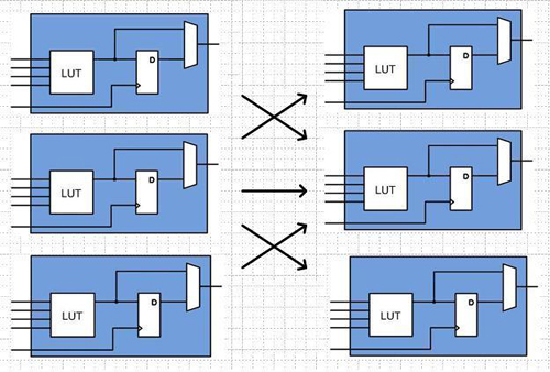
Figure 2: Programmable Routing Channels
The IOB features inputs and outputs signals of the FPGA chip, which support a variety of I/O signal standards like LVTTL, LVCMOS2, PCI, GTL,GTL+, HSTL Class I, HSTL Class III, HSTL Class IV,SSTL3 Class I and II, SSTL2 Class I and II,CTT and AGP-2X etc. These IO cells are shown in Figure 3.
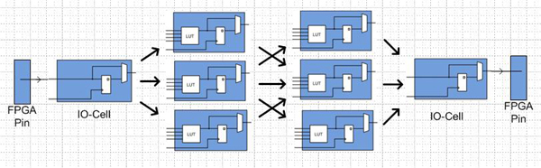
Figure3: IO Cells
In addition to general purpose routing resources, the FPGAs also have high speed dedicated lines in between neighboring logic cells. The most common type of high-speed dedicated lines is “carry chains”. Carry chains are particularly useful in implementing arithmetic functions like adders and counters with high efficiency, achieved through high operating speed and low logic usage.
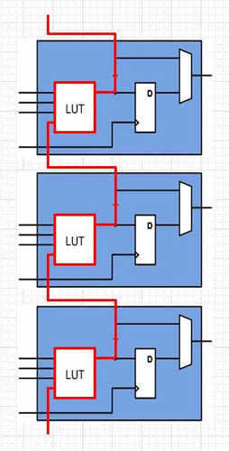
Figure 4: Carry Chains
In addition to logic cells, all new FPGAs are equipped with dedicated blocks of internal Static RAM. This Static RAM is distributed among and controlled by the logic elements. There are two types of internal RAMs in an FPGA: Block RAMs and Distributed RAMs. The size of the RAM needed in system design usually determines which type of RAM should be used.
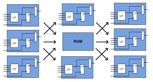
Figure 5: Internal Static RAM
Broadly speaking, FPGAs have two types of pins: “user pins” and “dedicated pins”. The user pins are usually called “user I/Os” which are user programmable and may be configured either as inputs, outputs or as bi-directional pins. Each IO pin is connected with the IO cell inside FPGA. Unlike user pins, the “dedicated pins” are hard-coded to dedicated functions like for power input, FPGA configuration and clock input etc. These pins can only be used for their dedicated functions.
In addition to the digital functions, some FPGAs are also equipped with analog features like programmable slew rate and drive strength on each output pin. Another common analog feature is differential comparators on input pins designed to be connected to differential signaling channels. A few mixed signal FPGAs even feature integrated peripheral Analog-to-Digital Converters (ADCs) and Digital-to-Analog Converters (DACs) with analog signal conditioning blocks thus allowing them to function as a system-on-chip.
FPGA Manufacturers
The internet sources claim that there are at least five companies in the world that involved with the manufacturing and fabrication of FPGAs. These companies are:
- Xilinx
- Altera
- Lattice
- Actel
- SiliconBlue
Among these companies Xilinx is the biggest name, as it invented the FPGAs in 1984 and may be deemed as global technology leader in the field of FPGAs.However, Altera is not a small name either. Statistics available on internet reflect that both Xilinx and Altera hold the major FPGA market share. As compared with the first two companies Lattice, Actel and SiliconBlue are small players.
How to choose an FPGA
Perhaps the most critical questions, while developing an FPGA based system, an embedded system developer may face are: how to choose an appropriate FPGA chip for his particular embedded application? And how large a device will he require to fit his design? There are many parameters and specifications that an embedded system developer should consider while choosing an FPGA chip, however, some of the most important parameters that an embedded system developer must consider, while examining the specification of an FPGA chip to choose and compare FPGAs for a particular application, are: configurable logic blocks like slices or logic cells, fixed function logic like multipliers, and memory resources such as embedded block RAM. The Table 1 given below shows resources specifications that may be used to compare FPGA chips within various families of Xilinx.
Table 1
|
|
Virtex- II 1000 |
Virtex- II 3000 |
Spartan-3 1000 |
Spartan-3 2000 |
Virtex-5 LX30 |
Virtex-5 LX50 |
Virtex-5 LX85 |
Virtex-5 LX110 |
|
Gates |
1 million |
3 million |
1 million |
2 million |
- |
- |
- |
- |
|
Flip-Flops |
10240 |
28672 |
15360 |
40960 |
19200 |
28800 |
51840 |
69120 |
|
LUTs |
10240 |
28672 |
15360 |
40960 |
19200 |
28800 |
51840 |
69120 |
|
Multipliers |
40 |
96 |
24 |
40 |
32 |
48 |
48 |
64 |
|
Block RAM (kb) |
720 |
1728 |
432 |
720 |
1152 |
1728 |
3456 |
4608 |
The number of logic gates that an FPGA chip is equipped with has traditionally been the most commonly used metric to compare the size and capacity of FPGA chip to ASIC technology. However, this parameter does not truly describe the features and components an FPGA chip is actually equipped with. This is why the Xilinx did not mention the equivalent number of logic gates for new Vertex-5 family of FPGAs.
According to Xilinx, there are three metrics that are defined to describe the FPGA device capacity: Maximum Logic Gates, Maximum Memory Bits and Typical Gate Range.
Key Benefits of FPGA Technology
The global market of FPGAs is growing at an enormously high rate and popularity of FPGAs is growing day by day. A unique feature of FPGA is that it combines the best parts of ASICs and processor-based systems. The most compelling advantages of FPGAs are very short time-to-market, low start-up cost, low financial risk and flexibility of updating the design as FPGAs are programmed and configured by the end-user. Some of the key advantages of FPGAs are:
- High Performance
- Short Time to Market
- Cost Effective Solution.
- Reliability
- Long-term Maintenance
A brief description of these key advantages of FPGA Technology is given below:
- Performance : Unlike Digital Signal Processors (DSPs) and Microprocessors, which execute the instructions sequentially, FPGAs are capable of executing instructions in parallel and thus exceed the computing powers of DSPs and Microprocessors by accomplishing more computation per clock cycle. Due to capability of parallel processing, the FPGAs can deliver many times the processing power per dollar of a DSP solution in some applications where performance and parallelism are important. This has also been established by Berkeley Design Technology Inc. (BDTI), which is a renowned analyst and benchmarking firm for embedded systems. Since inputs and outputs in FPGAs may be controlled at the hardware level, this helps provide faster response time and particular functionality so that the application requirements may be precisely matched.
- Short Time to market: In this competitive market the most challenging and the most important factor for an embedded systems developer, while delivering the end product to market, to consider is to meet the challenges posed by time-to-market. The embedded system developers are always under pressure to deliver the end product to market in as short time as possible. Under these circumstances, the FPGA Technology due to its flexibility and rapid prototyping capabilities offers a great support and relief to the embedded system developer in greatly reducing the product development cycle to deliver the end product to the market in a short time. As compared with ASIC design, an idea or concept may be tested and verified in hardware in no time without going through the long fabrication process of custom ASIC design. Incremental changes in a design concept may be implemented and practically tested on the FPGA chip within hours instead of weeks. The availability of Commercial off-the-shelf (COTS) hardware with different types of I/O already connected with user-programmable FPGA chip, has added great flexibility to FPGA based system development. It has helped greatly reduce the development cycle and hence it has also further reduced the time-to-market. With rapid advancement in FPGA technology, advanced software tools have also been made available to the embedded system developers which have remarkably decreased the learning curve with layers of abstraction. To facilitate the embedded system developer in rapid system development, the high-level software development tools for FPGAs often include valuable IP cores, which are prebuilt functions for advanced signal processing and control provided with the software.
- Cost: The cost of a technology greatly affects its popularity with engineers and system developers. The nonrecurring engineering (NRE) expense of custom ASIC design based solution is much too higher than FPGA-based hardware solutions. The ASIC design based solution costs lower only if the bulk production is done and this greatly brings down the unit cost. However, the problem with ASIC design based solution is that no changes or up gradation may be accomplished in ASIC design based solution, once the end product has been developed. Many end users need custom hardware functionality only for tens to hundreds of systems in development. System requirements often change over time, incremental changes and up gradations to FPGA-based designs can be made easily at negligibly a lower cost as compared with ASIC design based solution. The nonrecurring engineering expense of re-spinning an ASIC is stupendously high. Under these circumstances FPGA based design is a very handy solution due to its flexibility and re-configurability even after the FPGA chip has been installed in the end product.
- Reliability: Sophisticated software development tools for FPGAs provide programming interface for the embedded system developer to develop a code in Hardware Descriptive Language (HDL), while FPGA circuitry is a hardware realization of program execution. Several layers of abstraction are often involved with processor based system that help schedule different ongoing tasks and share resources among multiple processes. Hardware resources are managed by the driver layer, while the memory and processor bandwidth are controlled by the operating system. For any given processor core, whether it is Digital Signal Processor or general purpose microprocessor for PC, instructions are executed sequentially. Due to the sequential execution of instructions, processor based systems execute instructions on priority basis; a higher priority instruction may interrupt a lower priority instruction that is being currently executed. This may risk the reliability of the processor based system in time-critical applications. As compared with processor based system FPGAs provide much more reliable solutions where instructions may execute in parallel without any risk of higher priority time-critical instruction interrupting a lower priority instruction. Unlike processor based systems, FPGAs do not use operating systems and deterministic hardware resources are dedicated to every task. Thus FPGA based systems are supposed to be much more reliable than processor based systems particularly for time critical applications.
- Long-term maintenance: As has been discussed earlier, FPGA chips may be upgraded and reconfigured in the field even after the FPGA based product has been installed. As compared with redesigning an ASIC based hardware solution, the FPGAs are quite flexible and require much lesser time and much lower cost for reconfiguration and functional modifications. The typical example of a system where FPGAs may be regarded as the most desirable solution is digital communication protocols, where the specifications and parameters of protocol may change over time. In such as case the ASIC based hardware solution may cause forward compatibility and maintenance related issues. Since FPGAs are reconfigurable in the field, so they are flexible enough to keep up with the modifications and up gradations that might be necessary in future. As the system or end product matures functional modifications and up gradations may be easily made to the FPGA based hardware solution without any need to waste resources and time in redesigning hardware or modifying the board layout.
Applications of FPGAs
Application areas of FPGAs are quite diverse and wide ranging. Broadly speaking, major application areas of FPGAs are: Digital Signal Processing (DSP), video processing, software defined radio, control systems engineering, bioinformatics, aerospace and defense systems, computer vision, speech recognition and processing, medical imaging, computer hardware emulation, ASIC prototyping, reconfigurable computing and radio astronomy etc.
Traditionally, FPGAs are utilized in applications where the volume of production is small and development resources and expenses required for creating an ASIC for that low-volume application are prohibitively high.
With advancement in FPGA technology the areas of application of FPGAs are growing day by day. FPGAs are particularly suitable in applications or implementation of algorithms where parallel processing offered by the architecture of FPGA may be utilized to deliver high performance. Due to the inherent parallelism offered by the internal architecture and logic resources, FPGAs are capable of delivering high throughput even at low clock rates.
With advancement in FPGA technology and availability of sophisticated development tools application areas of FPGAs are growing at a very high rate and it is anticipated that in future this technology may even replace ASIC.
Summary
This article is a brief introduction to FPGA technology. This article discusses the internal architecture of FPGA chip, renowned manufacturers of FPGAs, the metric to choose an FPGA chip and key benefits of FPGA technology as compared with Digital Signal Processor and microprocessor and major areas of application of FPGAs.
References:


- Comments
- Write a Comment Select to add a comment
To post reply to a comment, click on the 'reply' button attached to each comment. To post a new comment (not a reply to a comment) check out the 'Write a Comment' tab at the top of the comments.
Please login (on the right) if you already have an account on this platform.
Otherwise, please use this form to register (free) an join one of the largest online community for Electrical/Embedded/DSP/FPGA/ML engineers:


