


VHDL tutorial - A practical example - part 1 - Hardware
Quick Links
- Part 1: VHDL tutorial
- Part 2: part 2 - Testbench
- Part 3: combining clocked and sequential logic
- Part 4: Creating a hierarchical design
- Part 5: A practical example - part 1 - Hardware
- Part 6: A practical example - part 2 - VHDL coding
- Part 7: A practical example - part 3 - VHDL testbench
In previous posts I described some simple VHDL examples. This time let's try something a little more complex. This is part one of a multiple part article. This is intended to be a detailed description of one of several initial designs that I developed for a client. This design never made it into a product, but a similar design was used and is currently being produced. As a considerable amount of work was put into this effort, I decided to share this design through this forum as opposed to burying it completely. This design was intended to be a data acquisition sub-system for a low power, hand held instrument.
This part focuses on the hardware design, including some of the VHDL definitions of the I/O characteristics of the CPLD part. Future entries will describe the VHDL logic of the CPLD, along with the simulations of the part.
As stated above, the final design ended up looking quite different, but this particular design was quite interesting to me, as it accomplished the stated requirements, but also provided some additional functionality that was a nice bonus. Before I get too far ahead of myself, let's look at the basic requirements.
The complete design for this instrument contained a few sections, but my part was the data acquisition logic. On one side there was a small μProcessor, which handled the keypad, LCD and other aspects of the user interface. This μProcessor would be interacting with my design and would be responsible for crunching the numbers on the data captured by the acquisition logic. On the other side there was a laser driver (with programmable high and low current settings) and a pair of photodiodes and associated preamps. In middle, was my part, the data acquisition engine.
The data acquisition engine has the following basic functions:
1) Provide for synchronous (with sampling, below) switching of the Laser diode between the high and low output levels (controlled by a dual channel ADC, programmed by the μProcessor using SPI) at an approximate rate of about 2 KHz.
2) Collect a burst of data, made up of packets of 16 evenly spaced samples, of 16 bits per channel (2) for each cycle of the Laser diode, for about 1 second.
3) Allow for various sample lengths ( ~1 sec, ~0.5 sec, etc.).
4) Signal the μProcessor with an 'end of collection' interrupt.
In addition to the above functions, the circuit needed to consume as little power as possible, as this was to be a battery powered device. During data collection, current draws of 20-40mA was accceptable. During idle operation, current draw should be less the 1mA (the lower the better).
Various approaches were considered, but in the end, it was decided to collect the samples locally into a SRAM device, then interrupt the μProcessor at the end of the cycle and allow the μProcessor to download the data and process as necessary. This would require about 128K bytes of storage, storing at a rate of ~ 1M bit/sec.
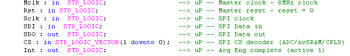
In addition to the above requirements, there was a need to minimize the interface to the μProcessor, as most of the pins were dedicated to other functions. Given this limitation the following interface to the μProcessor was defined:
- Mclk - Master Clock, 8MHz clock
- Reset - Active Low
- SCLK, SDI & SDO - SPI bus signals
- CS1 & CS0 - Chip select decode signals (to CPLD, ADC and serial SRAM)
- Int - Interrupt line to signal process complete (active high)
Of these signals, only Mclk, CS1, CS0 and Int are unique. The SPI bus lines and Reset were already assigned to work with other portions of the circuit. So, only four additional pins were required to provide an interface to the acquisition circuit. The Mclk signal (8MHz) was to be switchable, so that the data acquisition logic would go into a deep sleep (very low current draw) when not use.
The VHDL definitions for these signals are described as follows:
One of the compelling aspects of the hardware approach for this design, was the unique applications of some interesting components. For this design I found some relatively low-power components, that I don't normally use in my designs, along with some of my usual favorites (XILINX CPLDs). The following is a short description of the major component in the design.
- ADC - PCM1870 - 16-bit, low power stereo audio ADC. This device is used in many commercial devices, including portable audio players/recorders and cellular phones. Designed for audio, it provides sampling up to 50KHz, while providing a host of programmable features like: 30 db to -12 db gain, three-band tone control and high-pass and notch filtering. These were very compelling functions given problems in earlier designs of similar product with noise issues due to high power switching (laser) next to low level inputs (photodiodes). This device is controlled by the SPI bus (by the μProcessor via the CPLD) and sends out converted data via the I2S (Inter-IC Sound, Integrated Interchip Sound) bus, which is relayed to the SRAM (via the CPLD).
- SRAM - CY14B101Q2 - 1 MBit (128K x 8) serial SPI nvSRAM. This device acts a fast SRAM during data collection, but also provides a non-volatile storage using Quantum Trap elements (under program control or on power fail). The SPI timing for this parts runs up to 40MHz, providing write cycles of < 200 ns. The added non-volatile storage, while not needed for storing sensor reading, could be used for storing device setup and calibration data (nice added bonus). This device will be written to by the SPI bus (under command of the CPLD) and read from the μProcessor (via the CPLD)
- CPLD - XC2C64A - 64-macrocell, low-power, low-cost CPLD. This is one of my favorite parts, one that I have built several devices around. Small and fast, the flexibility of these parts is the reason that I keep coming back to them. This device will be programmed to function as an SPI bus peripheral (acquisition run length and run command) and as a SPI repeater (passing data to/from the ADC and SRAM). This device will also generate all of the necessary clocking and control lines (SPI and I2S) to run the acquisition bursts.
Given the major components, it is necessary to define the signal flow between the pieces. As the CPLD is acting as a SPI bus repeater (and sequencer) we will need another set of I/O pins for the internal (ADC/SRAM) SPI bus. This will include SCLK, SDI & SDO as well as chip selects for the ADC and the SRAM. The VHDL definitions for these signals are described as follows:
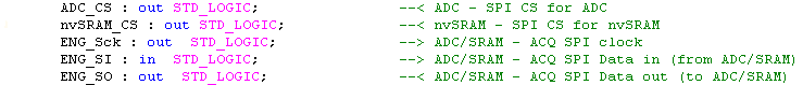
The ADC to CPLD interface is accomplished through the I2S bus. It requires only three signals in order to clock data from the ADC. The interface will be operated in the DSP or Slave mode where the CPLD will generate the LRCK (Left and Right clock) and the BCK (Serial bit clock), while the ADC will provide data through the DOUT (Serial audio data output) line. The VHDL definitions for these signals are described as follows:

The only remaining interface signal for the design is for controlling the Laser current. This is a digital signal that toggles the Laser current control between two programmed settings (0 for low power and 1 for high power). The VHDL definition for this signal is described as follows:
![]()
We will get back to the VHDL coding later, but we now have enough information to assign pins to the CPLD and generate a schematic body for the CPLD part which will become part of our final design. Here is schematic body for the Data Acquisition Engine CPLD:
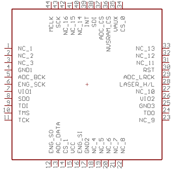
In addition to the previously defined pins there a series of pre-assigned pins that are needed to support the chip. These include power signals VIO1 (3.3V), VIO2 (3.3V), VCC (1.8V) and VAUX (3.3V), ground pins (GND1 GND2 and GND3) and the JTAG programming connections (TDI, TMS, TCK and TDO). Of the 44 pins on this device, there are 16 that remain unassigned (NC_1 to NC_16) based on the current assignments. This will allow some room for future growth, should there be remaining macrocells available after the design is coded and fitted.
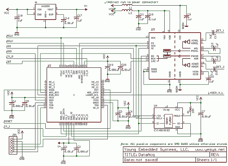
The only lose end at this point in the design is power. The overall design calls for 3.3V power, so the 1.8V supply, required by the CPLD, must be sub-regulated from the 3.3V supply. For this design, I used a MIC5253-1.8YC5, 100mA, low-noise, LDO regulator from Micrel to supply the 1.8V. The low quiescent current (75μA) and small footprint made this a good fit to the design.
With all the details in place we can complete the schematic diagram for the complete data acquisition sub-system. Signals to/from the μProcessor are shown on the left hand side, while signals to/from the Laser/photodiode module are shown on the right hand side. The completed schematic is shown below:
This pretty much completes the initial hardware design. The next steps will be to design the VHDL code needed to provide the desired functionality. This will be covered in the next part of this article. Hopefully this example has clearly demonstrated to the audience some of the steps needed to create a design based on complex programmable logic devices (CPLD).
Thank you for following along with me on this design example, I look forward to your comments, questions and suggestions, as I prepare the remaining parts of this article.
Good luck and happy designing!
Gene


- Comments
- Write a Comment Select to add a comment
To post reply to a comment, click on the 'reply' button attached to each comment. To post a new comment (not a reply to a comment) check out the 'Write a Comment' tab at the top of the comments.
Please login (on the right) if you already have an account on this platform.
Otherwise, please use this form to register (free) an join one of the largest online community for Electrical/Embedded/DSP/FPGA/ML engineers:


