


MyHDL FPGA Tutorial II (Audio Echo)
Introduction
This tutorial will walk through an audio echo that can be implemented on an FPGA development board. This tutorial is quite a bit more involved than the previous MyHDL FPGA tutorial. This project will require an FPGA board with an audio codec and the interface logic to the audio codec.
Review the Previous Tutorial
The previous MyHDL FPGA tutorial I posted a strobing LED on an FPGA board. In that tutorial we introduced the basics of a MyHDL module. To review, we described the hardware to control the LED.
The signal strobe is a periodic signal that strobes at the rate defined by the parameter LED_RATE. And the logic describes how the LEDs blink, in this case the led_bit_mem (a.k.a an enhanced shift register) will shift the 1 (the on bit) right or left depending on the current direction (state). In the LED example, a simple boolean is used to keep track of the state (direction).
After the design is verified with the original verification code. The design is run through the FPGA tools driven by Python scripts. The scripts and vendor tools generate and load the bit-stream onto a development board.
Note, these tutorials assume the reader is familiar with an existing HDL and/or will need to refer to the MyHDL manual. These tutorials implement a design and see it run on the FPGA and not an in depth guide to using MyHDL as a hardware description language.
Audio Echo
This example implements a simple echo by delaying the audio stream and adding the delayed signal with the non-delayed signal. The echo is implemented and tested with MyHDL and Python. The echo HDL description is then converted to Verilog. The Verilog is used as input to the FPGA vendor tool chain. The same as the previous example, the FPGA tool chain is driven by a set of Python scripts. The amount of delay in the echo is limited by the amount of embedded memory on the FPGA device.
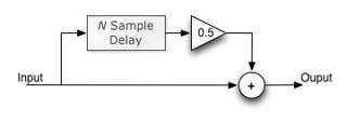
In this example the audio format used is 24bits @ 48000kHz. The implementation provides a parameterizable sample rate, sample width, delay (buffer depth), and the buffer word width. A greater delay can be achieved by limiting the number of bits saved in the buffer. As mentioned, the internal FPGA BRAM is utilized for the delay buffer. Depending on the device and the desired delay the internal memory can be consumed quickly. The amount of BRAM used determines the max delay. In this example only 16 bits are used in the delay path and the delayed signal is divided by 2 before adding to the non-delayed audio stream.
The following is the module interface and the parameter defaults.
Test Driven Design (TDD)
I want to emphasize the importance of testbenches and test driven development. For the echo, a straight-forward test can be defined. The test used generates a positive pulse followed by a negative pulse. The test will verify the pulses appear on the output at the expected delay. The following code snip demonstrates the capture of the output samples and the assertion that the delay (echo) was generated.
Full echo1 verification code is available on the bitbucket repository.
HDL Description in MyHDL
The following is the HDL description for the echo in MyHDL.
The design gets a new audio sample on each Fs strobe. On each new sample (at the sample rate, 48kHz) part of the sample is written to the BRAM delay buffer and a new delayed sample is retrieved. Then the BRAM "pointers" are incremented. The retrieved delay sample is combined (added) to the current input sample. Before the delayed sampled is added it is divied by two. The division by two is achieved with a shift operation.
Simulating the echo1 design will print some information on the configuration and resource usage. The following is the information printed when the design is simulated:
      Delay  ............................... 341.333333 ms
      Buffer word width .................... 16
      Scale factor ......................... 256 (8)
      Total Number Buffer Bits ............. 262144
      Number of Embedded Memory Blocks...... 16/ch (50.00%), xilinx.XC6S
      Number of Embedded Memory Blocks...... 16/ch (80.00%), xilinx.XC3S500E
      Number of Embedded Memory Blocks...... 15/ch (23.44%), lattice.ECP4-50
      Number of Embedded Memory Blocks...... 32/ch (44.44%), altera.EP4CE30
The output will print the approximate embedded memory usage given the parameters. A couple different devices were used as an example.
The following is a plot created by the testbench. It simply demonstrates that the input signal is output N samples later at half the amplitude.
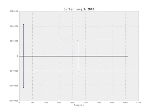
As discussed the testbench will verify that a simple input (pulse) will repeat given the expected delay. Additional plots were created from the testbench to visualize the delay. The following sine input it is visible that an additional sine (the delayed version) is added to the signal at the sample number equal to the buffer length.

The code examples are here.
But Wait ...
This post only discussed the HDL implementation, test, and simulation. The design wasn't loaded onto the FPGA board! The next post will have some results from running the design on a board. Stay tuned.
See the following post for the continuation of this example.


- Comments
- Write a Comment Select to add a comment
To post reply to a comment, click on the 'reply' button attached to each comment. To post a new comment (not a reply to a comment) check out the 'Write a Comment' tab at the top of the comments.
Please login (on the right) if you already have an account on this platform.
Otherwise, please use this form to register (free) an join one of the largest online community for Electrical/Embedded/DSP/FPGA/ML engineers:


