


Signed serial-/parallel multiplication
Keywords: Binary signed multiplication implementation, RTL, Verilog, algorithm
Summary
- A detailed discussion of bit-level trickstery in signed-signed multiplication
- Algorithm based on Wikipedia example
- Includes a Verilog implementation with parametrized bit width
Signed serial-/parallel multiplication
A straightforward method to multiply two binary numbers is to repeatedly shift the first argument a, and add to a register if the corresponding bit in the other argument b is set. The idea is similar to multiplication as taught in school, but a simple and-gate determines the product of two digits.
The processing delay largely equals the bit width, because each bit in b requires one accumulation step.
This can be an attractive compromise between cost and speed in the "mid-field": For example, at 100 MHz and a bit width of 20, the multiplier operates at around 5 MMUL/s. This is still quite fast e.g. for audio processing or similar applications that do not justify use of a hardware multiplier that will handle easily 20 times the throughput, but is a scarce resource on an FPGA. On the other hand, the serial-parallel multiplier is still 20 times faster than a completely bit-serial multiplier (which is otherwise very compact), and less complex to implement than more sophisticated algorithms like for example Booth encoding [1], which would handle multiple rows per iteration for the price of more hardware.
Wikipedia [2] gives an example for this algorithm but doesn't tell how it works ("for an explanation... see a computer arithmetics textbook"). A quick search on the web didn't turn up anything, and I ended up reverse-engineering the example with some help from [1], appendix A.
This article is the result, together with Verilog RTL code in the last section.
Adder width
As it turns out, an efficient implementation is a bit more involved than just shifting and adding. The output of the multiplier is twice as wide as the arguments. But, simply using a double-sized adder would result in a rather slow circuit, as the carry propagation through the adder sets the critical path.
The problem with signed numbers is the necessary sign extension to scale to the output bit width.
Figure 1 illustrates an 8-bit signed-signed multiplication.
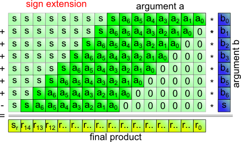
Figure 1: Signed-signed multiplication by repeated addition
Now how can we avoid the sign extension and use a shorter adder? The answer is, we extend by one bit only and add some temporary constant that guarantees a non-negative number. Later, we'll remove the sum of all constants from the result.
It's like a stage magician's trick: I first extend by one bit, then ignore it because I know it is zero. There are several seemingly unrelated things that fall into place at the end and poof, the frog turns into a toad.
Sign extension
For example, the MSB in an 8-bit unsigned number represents 128. For a signed number, the sign bit in the same place counts -128.
Let's look at some examples for two's complement numbers:
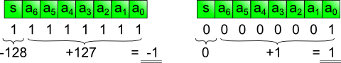
Figure 2: -1 and +1 as 8-bit two's complement numbers
Sign-extension by duplicating the sign bit keeps the value unchanged (figure 3):
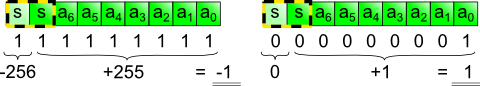
Figure 3: conventional sign extension to 9 bits
1-Bit extension to non-negative range
Now I flip the original sign bit, and put a zero into the extended sign bit (figure 4):
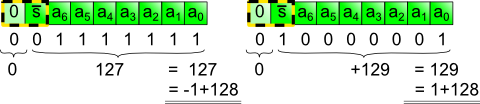
Figure 4: Sign bit inverted, and extended sign bit cleared
As can be seen, 128 was added in both cases, and a non-negative number resulted. In other words:
Modified partial products
The offset is now applied to the partial products, that is, the result of and-gating the shifted argument a with one bit of argument b.
Figure 5 shows the partial products and highlights all the bits that are changed to avoid sign extension. Effectively, a constant is added to each row. Note that the procedure always adds the same total offset to the result, regardless of input data.
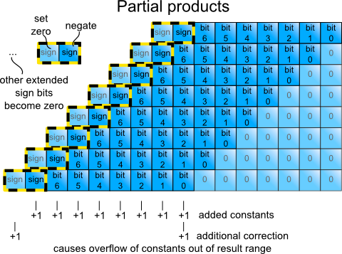
Figure 5: Bit changes to guarantee non-negative partial products
Adding two more bits, one at the low end and one at the high end of the correction range, will cause the sum of all constants to overflow and thus become zero (fig. 5, bottom). This is equivalent to subtracting the constants from the sum (by adding the two's complement).
Negating the final row
But this isn't all: So far we have not paid attention to the sign bit in argument b (fig. 1). As its weight is negative, the final row must be negated before addition.
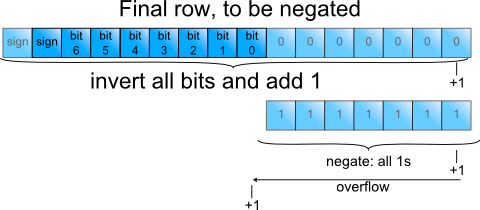
Figure 6: Sign-change of the last row
The low bits are introduced by zero padding and therefore known to be zero (figure 6), Inverting them and adding 1 would cause a single 1 to overflow into the active partial product bits. The same is achieved with less work by inverting only the active partial product bits, and adding 1 at their LSB (figure 7):
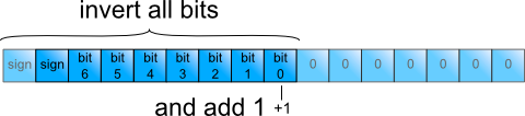
Figure 7: Simplified sign change in last row
Recap so far:
- Flipping the sign bit of every partial product enforces non-negative numbers by adding constants. This avoids sign extension and allows use of a narrow adder.
- Adding +1 to both the lowest and highest sign bit column causes the constants from the previous step to overflow and disappear from the result (no surprise here: The correction value is simply the two's complement of the constants added earlier)
- The final row is subtracted by inverting all active bits and adding 1 at the lowest active bit. Note, the sign bit was already inverted and is now changed back.
- Another 1 must be added at the lowest active bit of the final row as part of two's complement negation.
All constants combined
In other words, there are two +1s in column (x) (fig. 8) that overflow into a +1 at the next higher bit. It is conveniently included by changing MSB+1 in the first row (formerly extended sign bit, see figure 4) from 0 to 1 (y).
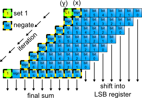
Figure 8: Calculation flow
Fig. 8 shows the flow of the calculation. Exceptions from conventional unsigned multiplication are marked. The adder requires only one bit more than the arguments.
Verilog implementation (download)
A Verilog implementation is included (links at bottom) that implements signed-signed multiplication as discussed. The bit width is parametrized, must be 3 or higher.
There is a testbench that exercises all possible input values. Note that the multiplier should work for any bit width, but exhaustive simulation for wide signals gets prohibitively slow.
Simulation with iverilog:
iverilog -DSK61LIB_INCLUDES -g2005 -Wall -o tmp tb_mul.v
vvp tmp -lxt2
The code works on ISIM from Xilinx ISE 14.7 webedition.
A quick synthesis trial on a Spartan 6-slx9 with a PN source gave 159 MHz as maximum clock speed. Using two separate adders instead of muxing one (see comments in code) raises this to 237 MHz but uses more slices. If speed is not an issue, try a different FSM encoding for state (i.e. "compact") for a slightly smaller design.
'x' assignments are used diligently as they make simulation results more readable, support optimization and help to spot conceptual errors (fig. 9).
For a bit width of n, execution takes n+2 cycles. This could be improved to n or even n-1 by using more complex control logic. The main "selling arguments" for the implementation as it is are maximum clock speed and simplicity.
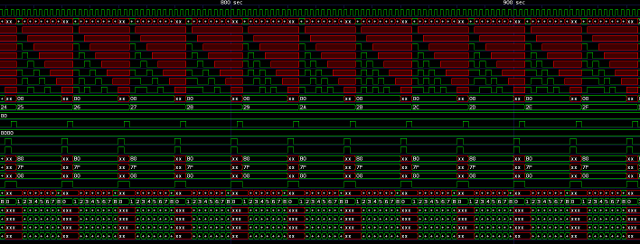
Figure 9: Simulation
Link: Verilog source code Link: Formatted source code (PDF) Link: testbench Verilog source code
References
[1] Fast Multiplication: Algorithms and Implementation: Doctoral thesis, Gary W. Bewick, 1994


- Comments
- Write a Comment Select to add a comment
To post reply to a comment, click on the 'reply' button attached to each comment. To post a new comment (not a reply to a comment) check out the 'Write a Comment' tab at the top of the comments.
Please login (on the right) if you already have an account on this platform.
Otherwise, please use this form to register (free) an join one of the largest online community for Electrical/Embedded/DSP/FPGA/ML engineers:


