


Fit Sixteen (or more) Asynchronous Serial Receivers into the Area of a Standard UART Receiver
Introduction
This article will describe a technique, available in many current FPGA architectures, to fit a large amount of logic into a small area. About ten years ago now (Feb/Mar 2005), I helped develop a multi-line Caller ID product. The Multi-Channel Asynchronous Receiver (MCAR) FPGA core developed for that product will be used to illustrate the technique(s) needed to fit a 16 channel MCAR into a single Spartan II XC2S30-5VQ100 FPGA.
To stay true to the original design, I will only describe the technique in terms of the capabilities of the FPGAs originally used to implement the project. Using more recent FPGAs architectures, the technique which will be described can now yield a quadrupled implementation, or 64 asynchronous receivers in the area of a single standard UART receiver.
The Problem
A multi-line Caller ID product is available in two configurations: (1) an 8-line unit, and (2) a 4-line unit. However, many customers needed a solution for more than eight lines, but less than 16 lines. Therefore, using the daisy-chaining capability of the units, customers would frequently buy an 8-line unit and a 4-line unit to support Caller ID on 10-12 incoming lines. However, many customers expressed displeasure at the cost of the two unit solution.
The Solution
The decision was made to provide a single 12-line unit. The extra RJ11 jacks needed would fit within the available panel space of the 8-line unit, but the large number of discrete parts needed to implement that number of Caller ID channels in the current products would not fit on the available printed circuit board area of the 8-line unit. After considering various options used on other projects such as multi-channel UARTs and microcontrollers with multiple serial ports (Dallas Semiconductor 80C320 microcontroller, AMD Am188ER microprocessor, and NXP LPC213x ARM microcontrollers), the decision was made to use a small Spartan II FPGA (XC2S30-5VQ100) and an NXP LPC213x ARM processor.
An SSP slave interface between the Spartan II FPGA and the LPC213x ARM processor would provide a low-pin count, fast interface to retrieve the Caller ID information that the MCAR would collect from the 12 Holtek Caller ID devices. The remaining challenge is how to implement at least twelve asynchronous serial receivers and miscellaneous power control logic for the Holtek Caller ID interface device.
The Spartan II XC2S30-5VQ100 FPGA only has 864 logic cells which consist of 1 4-input Look-Up-Table (LUT) and a FF/Latch. ( Note: Xilinx's definition of what constitutes a Configurable Logic Block (CLB) varies according to the FPGA family. For the Spartan II family, two logic cells are combined into a slice along with some additional multiplexers and dedicated arithmetic support logic. Further, two slices are combined into a CLB. Thus, a Spartan II CLB contains the equivalent of 2.25 4-input LUTs and two FFs/Latches. Unlike the logic cells in CLBs of more recent FPGA offerings, the logic cells comprising a Spartan II CLB are all of the same type.) As shown in Table 1 below, a single UART would require a significant portion of the available logic cells in the selected FPGA:
|
Module |
Slices | Slice Reg | LUTs | LUTRAM | BRAM |
| [-] M16C5x/ | 169/1154 | 24/580 | 71/1255 | 0/210 | 3/3 |
| [+] CPU | 252/405 | 116/202 | 306/488 | 40/40 | 0/0 |
| [+] SPI | 7/99 | 8/75 | 0/135 | 0/34 | 0/0 |
| [-] UART | 0/481 | 0/279 | 0/561 | 0/136 | 0/0 |
| SSP_Slv | 51/51 | 37/37 | 28/28 | 0/0 | 0/0 |
| [+] UART | 160/430 | 81/242 | 193/533 | 0/136 | 0/0 |
The particular UART referred to in the table is one which I've created to support an RS-232 four wire (plus ground) interface or an RS-485 two wire (plus ground) interface. The UART does support some advanced features such as receive timeouts and Rx/Tx FIFOs, but otherwise, it is a fairly stripped down relative of the 16550-compatible UART that I typically employ. This UART's receiver requires more logic to implement than its transmitter. But for the purpose of this analysis only, let's assume that a single receiver requires only (533+136)/2 = 335 LUTs and 121 registers to implement. (Note: the UART referenced in Table 1 includes an SSP slave interface. The initial SSP slave interface developed for this product to interface the ARM to the FPGA has proven to be a good low pin count way to interface FPGA-based peripherals to various microcomputers over the years.)
With only 864 logic cells available in the Spartan II FPGA, how will it be possible to implement 12 to 16 asynchronous serial receivers?
The answer to that question will be the subject of the remainder of this article. To adequately present the technique(s) employed, this will be a long article.
The Multi-Channel Asynchronous Receiver (MCAR)
The key concept to embrace is that the LUTs of many SRAM-based FPGAs may be written to synchronously. Although the LUTs in SRAM-based FPGAs are used to implement the combinatorial logic of a design, they may also be used for storage. As discussed in my previous article, "Use Microprogramming to Save Resources and Increase Functionality", synchronous FIFOs can be easily constructed using the writeable LUTs of SRAM-based FPGAs. In addition to that use, it is also possible to use the LUTs in the Spartan II FPGA to implement multiple shift registers, baud rate generators, state machines, distributed RAM FIFOs, and Block RAM FIFOs.
These components are all required to implement an asynchronous serial receiver. However, if those elements are implemented using the FFs of the FPGA's logic cells, the resources required for the 12 asynchronous serial receivers needed for this project would soon fill the selected Spartan II FPGA. By using the speed of the FPGA relative to the speed of the asynchronous serial data, it is possible to time multiplex the elements of a UART and support many more asynchronous serial receivers in the FPGA than would normally be expected.
Using a simple 4-bit counter which provides the "address" of a UART receiver channel and storing all of the needed data within the addressable bit cells of the FPGA's logic cell LUTs will allow the FPGA to easily pack 16 asynchronous receivers. As a matter of fact, enough logic resources will remain that it would be possible to also pack 16 asynchronous serial transmitters into the remaining resources. There wasn't a need to include that capability into the FPGA, so the 16 asynchronous serial transmitters were never actually included in the product.
I use 16 as the number of channels to implement for several reasons:
- it is a power of two;
- it matches the number of addressable elements in a Spartan II LUT;
- and it makes it easy to select an oscillator for baud rate generation.
Although the Holtek part outputs the Caller ID information at 1200 baud, I had every intention of using the MCAR core to be developed in this project in the future. Therefore, I wanted the baud rate generator to support standard rates and references. Thus, I chose to implement this project using a 29.4912 MHz oscillator. At this frequency, with a division by 16 to account for the sixteen channels, and another divide by 16 to account for the sampling rate of standard UARTs, the maximum baud rate is 29,491,200/256 = 115200 bps. I deemed this acceptable for virtually all applications for which I might want to use this MCAR. Furthermore, at a baud rate of 1200, only an 8-bit divider would be required: 115200/96 = 1200.
With the preliminaries specifications settled, it is necessary to define the components required for each receiver channel:
- input data register
- input data filter
- receive state machine
- baud rate generator
- data shift register
- output data holding register
For each of these elements of the receiver, it is a continuously running 4-bit counter that selects each channel's elements/components. Each of these elements will be discussed in the following subsections in their multi-channel configuration.
Multi-Channel Input Data Register
Each succeeding generation of the FPGAs has improved the hardness of its FFs against metastability. The registers recover faster and operate faster. The following statement is a hard lesson to learn, and it certainly not a lesson that should be learned while on a tight deadline: synchronize all inputs. This is especially true in this product where the serial outputs from the Holtek Caller ID chips can be guaranteed to be asynchronous to each other. Therefore, unless you just insist on processing noise, i.e. random characters, register each of the serial inputs with at least one FF.
The Spartan II FPGA has I/O block (IOB) FFs that you can use for this purpose. ( Note: virtually all FPGAs have this feature. To the best of my recollection, only the short-lived Xilinx 5200 FPGA family did not have IOB FFs.) In the schematic implementation that I used for the original project, I simply used the IOB FF library elements to accomplish the synchronization of the serial inputs to the clock signal used within the FPGA. In an HDL implementation, I would simply run all of the inputs directly into a FF, and set the place and route tools to place these initial FFs in the IOBs. In some flows, you can still instantiate the IOB FFs directly, so that approach is also an option.
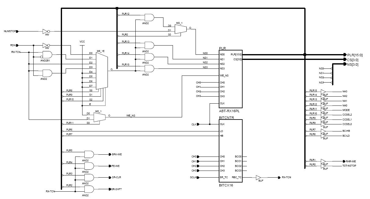
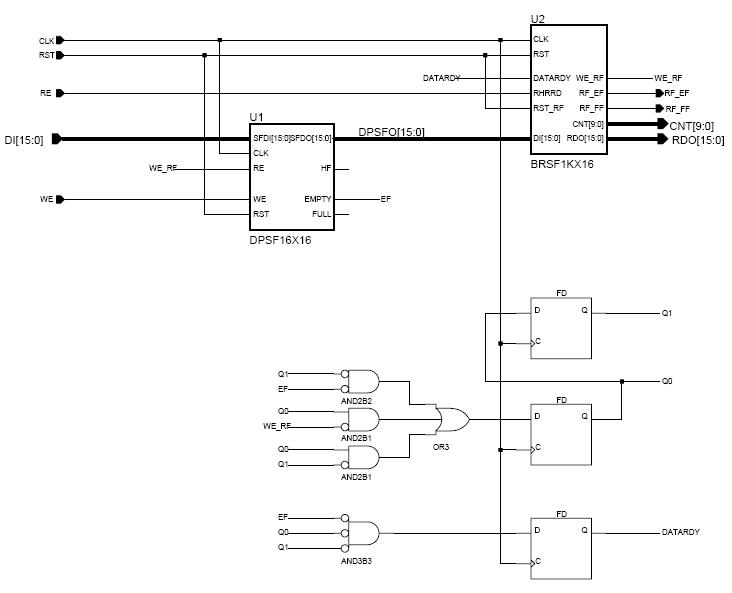
MCAR Top-Level Block Diagram Description
The preceding subsection discusses the need for synchronization registers on each of the asynchronous data inputs into the Multi-Channel Asynchronous Receiver (MCAR). Figure 1 provides a block diagram of the MCAR that will be described in greater detail in the following subsections of this article.
Figure 1: Multi-Channel Asynchronous Receiver (MCAR) Top-Level Block Diagram.
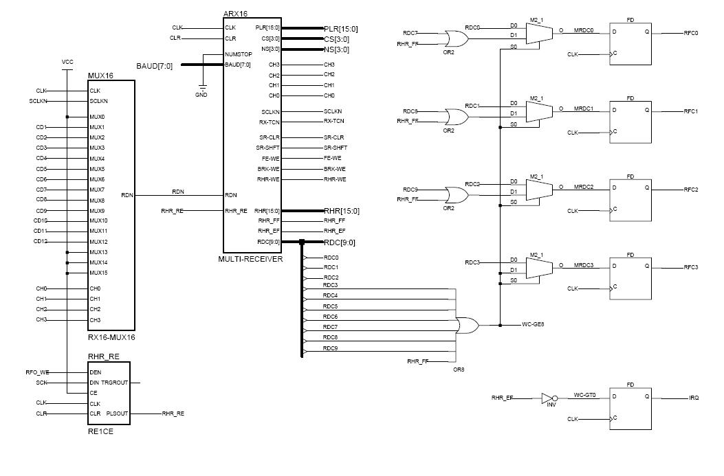
The MCAR is being developed as a general purpose component for future use, but notice that only twelve of the input data channels are being used. That is specific to the Caller ID application described above, and has no effect on the overall implementation. Further notice the application specific FIFO word count logic included in the upper right of the diagram.
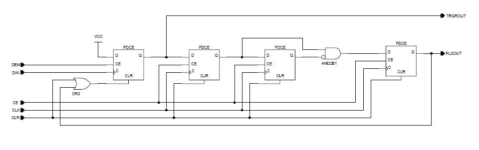
In the lower left of the diagram is a clock domain crossing circuit that I use for whenever I have to detect edges of signals generated in two different clock domains. In the case of this specific application of the MCAR, the ARM microcontroller and the FPGA are considered to be on two different clock domains. Figure 2 below is a representation of the RE1CE function.
Figure 2: Clock Domain Crossing Edge Detector.
Multi-Channel Input Data Filter
The RX16-MUX16 module in Figure 1 is the MCAR's channel data multiplexer and the multi-channel input data filter. I use a data filter in all of my UART designs. It is not particularly complicated, but it filters out impulse noise that can sometimes occur on serial interfaces due to bad grounding, electromagnetic interference, etc. If any of you have ever used the UART of an 8051 microcomputer in a noisy environment, you're likely to have experienced receiving random data. The start bit synchronization of that UART core is faulty, and it simply detects the falling edge of the start bit and does not verify it at the mid-bit point. In a noisy environment, noise pulses on the receive data of that UART can trigger a receive cycle even when the line is functionally in the idle or mark state.
Thus, since I started building my own UARTs into FPGAs, I've used a 3 sample majority voting circuit to determine the state of the receive data. With only 3 inputs, the logic needed to implement this filter is guaranteed to be fit into a single 4-input LUT of the FPGAs that I use in my designs. Although, in schematic form the filter circuit appears to be complicated, the synthesizer collapses it into a very compact representation in the FPGA's LUTs.
Figure 3 below provides a schematic of the implementation of the data filter that I use. For the Multi-Channel Input Data Filter to operate reliably, the input data supplied to it must be synchronized by the Multi-Channel Input Data Register discussed above.
Figure 3: Multi-Channel Input Data Filter.
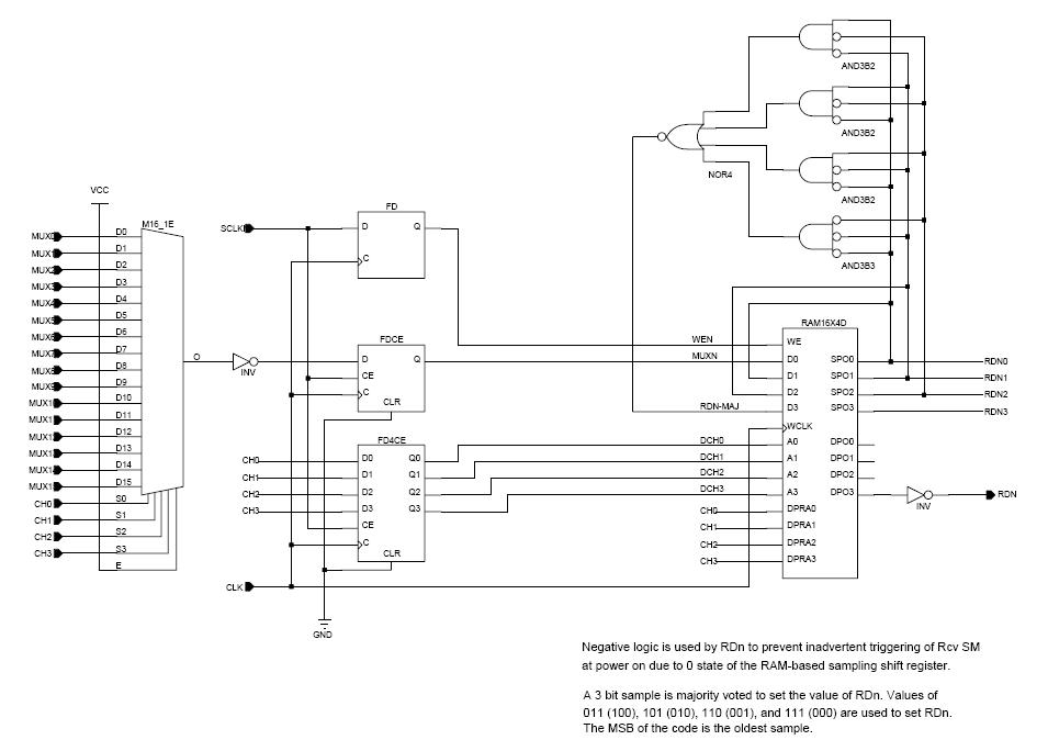
Logic 0 is the normal condition of FFs and RAMs in the FPGA following configuration. Without resorting to some contortions with default parameters in the schematic implementation shown, the default condition would cause the receiver logic to detect a start bit immediately after configuration. To avoid all of the complexity needed to correct the default conditions in the dual-port RAM and the FDCE delay FF above, I simply decided to use inverted logic. That is the reason for the inverter at the input and the output of the module. It is also the reason for the NOR4 gate in the majority logic circuit.
The input data from the Multi-Channel Input Register are multiplexed onto a single line, inverted and registered. The FDCE FF holds the new sample for that particular channel at 1/16 of the baud rate for that channel. The signal SClk is the 16x sample clock for the channel selected by the Ch[3:0] code. The channel code is also registered. If SClk is not asserted, then the channel input data register is not sampled, and neither is the 4-but input data filter shift register represented by the 4-bit dual port distributed RAM. The fourth bit, or most significant bit of the RAM, is the majority logic level of the preceding three samples of the channel's input data register.
Input data patterns {0, 0, 0}, {0, 0, 1}, {0, 1, 0}, and {1, 0, 0} are voted as logic 0 (logic 1 in the active low circuit of Figure 1), and input data patterns {1, 1, 1}, {1, 1, 0}, {1, 0, 1}, and {0, 1, 1} are voted as logic 1 (logic 0 in the active low circuit of Figure 1). Since the receiver only sees the output of this filter circuit, there's no problem in correctly processing each channel's receive data input, RDN, where the N represents channel number and not polarity. ( Note: I've adopted the convention of a leading N/n to indicate polarity. Further, I also adopted the convention that all signals should be active high within my logic. I recommend these conventions to all.)
MCAR State Machine
Figure 4 illustrates the internal block diagram of the MCAR's functions except for its channel multiplexer and input data filter module.
Figure 4: Internal Block Diagram of Multi-Channel Asynchronous Receiver.
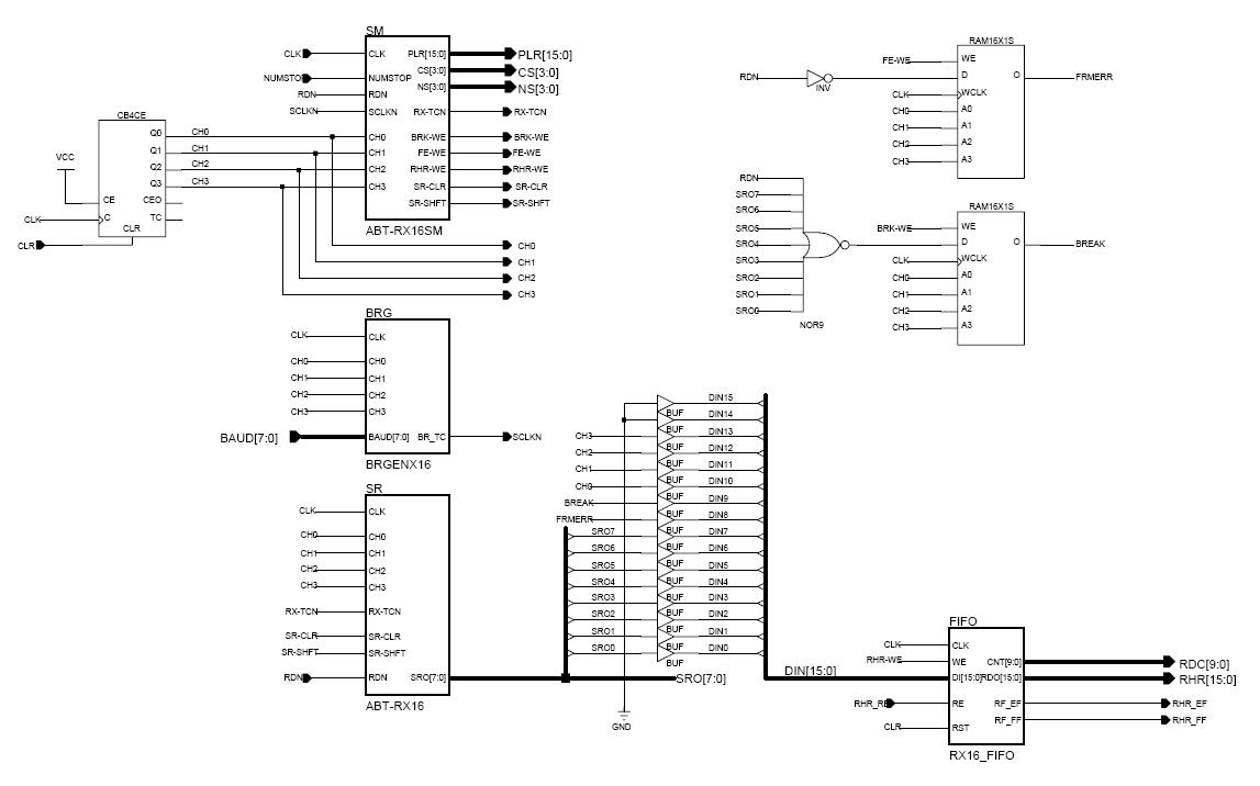
In the top left is found the free running 4-bit counter that generates the channel select code that drives all of the multi-channel elements of the MCAR. In the top right are the multi-channel "registers" for the framing error and and break error conditions. In the bottom right is the multi-channel receive data holding register (RX16_FIFO), which is implemented with an expanded version of the RTFIFO which was the subject of my previous article.
In the lower right portion of the center of Figure 4 is the circuit that merges the channel select code and the corresponding data and error conditions as the data to be written to the multi-channel receive data holding register. Along the left portion of the center of Figure 4 are the modules for the multi-channel state machine (RX16SM), baud rate generator (BRGENX16), and receive data shift register (RX16).
Like the multi-channel framing error and break error "registers", each channel of the MCAR could have been provided a different baud rate. Since all of the Caller ID chips operate at the same baud rate, only a single baud rate value is provided to the multi-channel baud rate generator. This is not a limitation of the MCAR, but simply an application-specific optimization that was made for the project being used to illustrate the MCAR.
Pushing into the RX16SM module shown in Figure 4 provides a view (see Figure 5 below) into the operation of the MCAR's state machine.
Figure 5: Multi-Channel Asynchronous Receiver State Machine.
As depicted in Figure 5, the MCAR's state machine resembles the microprogrammed state machine described in my previous article: " Use Microprogramming to Save Resources and Add Functionality". If you are not comfortable with microprogramming as structured implementation technique for state machines, the referenced article should be consulted. In this article I will not be discussing the technique in depth, and will simply define the control fields and special features that are pertinent to the operation of the state machine.
The following vector defines the microprogram word of the MCAR's state machine:
PLR[15:0] = {NS[3:0], Mode, CCSel[2:0], BC_HB, BC_LD, BRK_WE, FE_WE, SR_Clr, SR_Shft, RHR_WE, TstNStop}
The NS field controls the flow through the state machine. It defines the value that will be stored in the multi-channel current state register. The CCSel field provides the control for control whether CS is loaded with NS or not. If NS is not loaded into CS, then CS is unchanged and the SM remains in its current state. The TstNStop control bit will select one of two states in order for the SM to process one or two stop bits.
The Mode bit controls the rate at which the SM operates. While looking for the falling edge of the start bit, the Mode bit selects the system clock as the update clock. This allows fast detection of the falling edge of the start bit, which is being sampled in the multi-channel input data filter module at a rate corresponding to 16x the baud rate of channel. After the falling edge of the start bit is detected, the Mode bit select the bit rate, but the first load value, controlled by BC_HB, puts the bit sample point at the mid-bit point. If the start bit is verified by the SM, then the reload value is set to a full bit delay which then samples the 8 data bits and the one or two stop bits at their mid-bit point as well.
The channel select counter selects the input data, the CS, and the bit count registers for each channel. Each channel can be in a different state. The baud rate generator supplies the SClk signal to the bit counter, so each channel can also be operating at different speeds. Although the SM is fairly simple, the microprogrammed implementation included in this implementation provides a very compact way of sharing the resources among the sixteen channels supported by the design.
Figure 6 and Figure 7 show the implementation for the multi-channel pipeline register and the multi-channel bit counter modules, respectively.
Figure 6: Multi-Channel Pipeline Register (and Microprogram ROM) Module.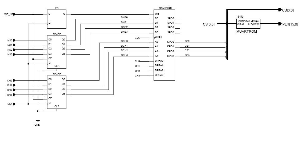
Figure 7: Multi-Channel Bit Counter Module.
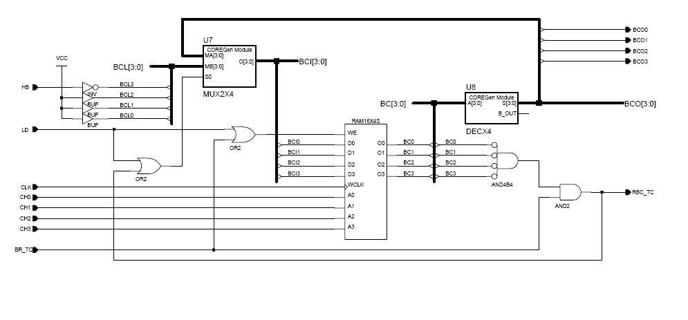
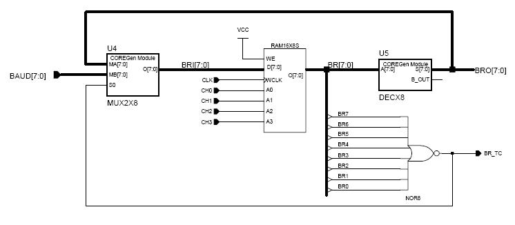
Multi-Channel Baud Rate Generator
The multi-channel baud rate generator is implemented simply with a multi-channel counter register and shared decrementer, 2:1 multiplexer, and identity comparator. A diagram of the multi-channel baud rate generator is provided by Figure 8.
Figure 8: Multi-Channel Baud Rate Generator.
Multi-Channel Output Data Register
There exists a potential for all sixteen channels to complete within the same cycle. Although this situation is unlikely given the asynchronous nature of the telephone system as well as other variables, the probably that this condition may occur requires that we store the output data for each channel in a FIFO capable of accepting data and storing in a single clock cycle. After storing it in such a FIFO, additional circuitry, not part of the MCAR, can pull it out and redistribute it to individual FIFOs for each channel, or it can simply buffer it in a large block RAM FIFO.
For the Caller ID application, it is the second option that was chosen. There is ample memory in the attached ARM processor, and it is certainly fast enough to read the Block RAM FIFO and demultiplex each channel's data into its own queue. As pointed out in Figure 4 above, each character received by the MCAR is stored as a 16-bit value in the output data register. The 16-bit value written includes the channel number, the framing and break error bits, and the eight receive data bits. This format allows the ARM to process each character received, and store it in a dedicated queue for each channel. Figure 9 below is a diagram of the MCAR's output data register.
Figure 9: Multi-Channel Output Data Register.
Summary
The preceding sections have demonstrated using the RAM cells of a Spartan II PFGA as compact storage in order to support a sixteen channel MCAR in a low density FPGA. In addition to using LUTs as register arrays, the SM was microprogrammed, stored in a read-only array of LUTs, and shared between all of the channels. Both techniques were required to successfully implement the MCAR in the XC2S30-5VQ100 target.
Table 2 below summarizes the complete logic required to implement the MCAR, the RTFIFO, the SSP Slave interface, and the Holtek Caller ID power control circuits. The entire project, not just the MCAR, easily fit into the target FPGA, and there were sufficient resources available for additional functionality if that ever became necessary.
| Resource | Utilization |
| Number of Slices | 273/432 |
| Number of FFs | 167/864 |
|
4-input LUTs
|
308/864 |
|
Dual-Port RAMs (2 LUTs/DPRAM)
|
21
(42) |
|
16x1 RAMs (Single Port RAM) (1 LUT/SPRAM)
|
35 |
| Number of Block RAMs | 4/6 |
|
Total Equivalent Gate Count for Design
|
76,173 |
Interestingly, the 308 LUTs and 167 FFs needed to implement the complete Caller ID project in the Spartan II are remarkably close to the number estimated at the beginning of this article using a standard Verilog HDL implementation of a serially connected (SSP), buffered UART (64 byte FIFOs for receive and transmit).
Although technological progress has rendered the Caller ID product obsolete in today's world, the techniques used to successfully implement a 12-line Caller ID unit are still applicable today. Microprogramming, using either the LUTs or the Block RAMs, is a powerful design approach/methodology. Extra-ordinary use of the LUTs as demonstrated by the MCAR can be applied, together with microprogramming, to significantly increase the number of functions that can be embedded in an FPGA.
Taking advantage of these two techniques may make the difference between producing a cost-competitive product or not. FPGAs continue to decrease in price and increase in capacity, but the unit cost of FPGAs is not always aligned with the price with the expected/anticipated sales quantities of a product. The technique(s) that I've discussed in this article were the only viable way to use an FPGA and an ARM to replace a large number of small microcomputers and discrete logic in a cost competitive manner.
I welcome any positive comments or questions regarding the subject of this article, or previous related articles.
What's Next
Over the past few years I have developed a number of applications using microprogramming at a level of complexity significantly greater than that demonstrated by the microprogrammed state machines in the MCAR and RTFIFO. My next article will describe my re-implementation of the Fairchild Semiconductor F9404 Microprogram Sequencer. Even though the 9408 is relatively simple, it provides several features that allow the implementation of very sophisticated state machines. I will use it in future microprogramming articles.
© 2015 Michael A. Morris, All Rights Reserved.


- Comments
- Write a Comment Select to add a comment
Hi Michael. I was wondering if you had had a chance to convert this to verilog as you suggested in your previous post on the FIFO implementation.
It would be very useful for me.

jmfoed94:
Yes I have a Verilog version of the project. I have not decided under what license to release it under at this time. At this point, I am leaning toward using the GPL 3.x series of licenses. If that is acceptable, then I may have time later the week to make the appropriate changes to the source and release the project on my Github account.
Michael A. Morris
That would be great. I'm working at the University of Arizona on an adaptive optics research project. I'd be delighted to incorporate some of your work if possible. I have a xilinx design with 336 uarts in it. It's a routing and timing nightmare and this mcar design is just what the doctor ordered.
I'm also interested in your generic microprogramming work for building state machines. I did a microprogramming course back in ~1980 on a Univac 1100 where I built a 6800 chip in microcode. I was digging through my old textbooks looking for the microprogramming text this morning. I fear I have given it away, though!
Thanks for sharing your knowledge and your projects with the world!
John
jmford94:
I didn't get around to packaging up the code for release this weekend.
I did review the test bench I generated for testing the implementation, and it appears to test that the implementation is performing as desired. I re-ran the synthesis for an Artix-7, and it appears to successfully place a 16 Asynchronous Receiver version into the part with a 230 MHz constraint without too much trouble.
This should be sufficient to support an asynchronous data rate of about 1.024 MHz for 15 channels using a 16x oversample. If you need a higher rate, you can change the oversampling, reduce the number of channels scanned, or some combination of both.
Go to my public GitHUB account, https://github.com/MorrisMA, locate my email address in the GPL headers of one of my publicly released projects, and send me an email. I'll send you a zip of the project. This will have to do for the time being until I have time to release the project on GitHUB.
To post reply to a comment, click on the 'reply' button attached to each comment. To post a new comment (not a reply to a comment) check out the 'Write a Comment' tab at the top of the comments.
Please login (on the right) if you already have an account on this platform.
Otherwise, please use this form to register (free) an join one of the largest online community for Electrical/Embedded/DSP/FPGA/ML engineers:


