


VHDL tutorial - A practical example - part 2 - VHDL coding
Quick Links
- Part 1: VHDL tutorial
- Part 2: part 2 - Testbench
- Part 3: combining clocked and sequential logic
- Part 4: Creating a hierarchical design
- Part 5: A practical example - part 1 - Hardware
- Part 6: A practical example - part 2 - VHDL coding
- Part 7: A practical example - part 3 - VHDL testbench
In part 1 of this series we focused on the hardware design, including some of the VHDL definitions of the I/O characteristics of the CPLD part. In part 2, we will describe the VHDL logic of the CPLD for this design.
With any design, the first step to gather the requirements for the job at hand. From part 1 of this article, I have copied two sections that address some of the requirements for the CPLD design.
The data acquisition engine has the following basic functions:
1) Provide for synchronous (with sampling, below) switching of the Laser diode between the high and low output levels (controlled by a dual channel ADC, programmed by the μProcessor using SPI) at an approximate rate of about 2 KHz.
2) Collect a burst of data, made up of packets of 16 evenly spaced samples, of 16 bits per channel (2) for each cycle of the Laser diode, for about 1 second.
3) Allow for various sample lengths ( ~1 sec, ~0.5 sec, etc.).
4) Signal the μProcessor with an 'end of collection' interrupt.
and
This device will be programmed to function as an SPI bus peripheral (acquisition run length and run command) and as a SPI repeater (passing data to/from the ADC and SRAM). This device will also generate all of the necessary clocking and control lines (SPI and I2S) to run the acquisition bursts.
Also from part 1, we can assemble the fragments of the device I/O description of our CPLD device into a complete entity.
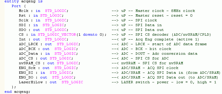
The two CS lines are used to decode the selected SPI target for communications handled by the CPLD. There are three targets associated with the design; the internal peripheral, ADC and nvSRAM (note: the two external targets, ADC and nvSRAM are defined such that CS(1) is zero, this will simplify some of the logic when decoding the chip selects and SPI implementations). The final CS line combination ("11") represents the 'No select' case. This is used when other devices in the overall design are targets of a SPI transaction. The following assignments are made in regards to these lines:
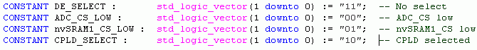
With the major aspects of the acquisition engine logic described, we can form a logic block diagram to assist in the process of flushing out the details of the functional areas.
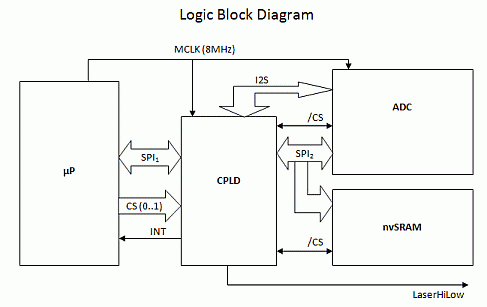
Now we need to look at the timing of the SPI and I2S buses in order to better understand the VHDL implementations of these buses. To start with, we will look into the SPI timing. Both the ADC and the nvSRAM use the same basic timing (the ADC has no read back, so the SO is always tri-stated). Both devices sample the SI line on the rising edge of SCK. The nvSRAM has output data (SO) ready to be sampled on the rising edge of the SCK. In order to simplify the design, the internal SPI peripheral of CPLD will be coded with the same timing. The internal SPI peripheral will utilize the SO output to send back the run status of the acquisition engine. All eight of the status bits will be set to the current state of the Run signal.
The internal SPI peripheral command set will consist of a single register, containing a run flag and a run length variable. The run length variable (CycleCnt) is used to set the duration of the acquisition engine run. The internal variable is configured to eleven bits, allowing a range of 1 to 2048 Laser cycles. Only the upper seven bits of this variable are settable through the SPI register allowing for run lengths of 16 (0x00) to 2048 (0x7F), in multiples of 16.
![]()
A part of the function of the acquisition engine is to direct the data from the ADC (in I2S format) to the nvSRAM (in SPI format) during the course of the data burst. In order to accomplish this, the nvSRAM needs to be configured to receive data prior to starting the data burst. The CY14B101Q2 datasheet describes the 'Burst Mode Write', sequence as a means to write to consecutive addresses within the SRAM, which sound like the right mode for this design. The process involves selecting the device (CS set low), transmitting the WRITE instruction, starting address and multiple bytes of data, while holding the CS line low. The WRITE instruction is '0000 0010b', the starting address is a 17-bit quantity, with 7 bits of leading zeros, for a total of 24 bits. This is followed by a continuous stream of data, which is read off the ADC. For simplicity, we will use a starting address of zero, so our setup stream becomes 6-'0's, followed by a single '1' and then 25 more '0's (for a total of 32 bits). Details, like making sure that the device is write enabled (WREN instruction) are left to the μProcessor, to be handled prior to starting a data collection cycle, as these actions will persist outside of a chip select sequence (and handling them in a pass through mode from the μProcessor will greatly reduce the complexity of the CPLD design).
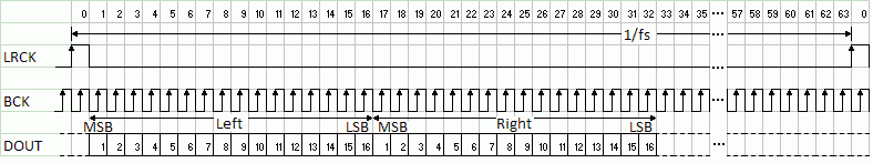
With the SPI actions specified, let's move on to the I2S bus. The PCM1870 uses the I2S bus to transmit the converted data off the device. There a few different modes for this bus, which determine the source of various clocks and the format of the output data on the DOUT pin. For this design, the simplest approach is for the CPLD to generate all of the clocking signals. For this reason, this design will use the DSP format for the I2S bus (LRCK and BCK are inputs to the ADC). The setup of the DSP mode and all other aspects of the ADC setup will be left up to the μProcessor, to be handled prior to starting a data collection cycle. All that the CPLD will need to do during a data collection cycle is to generate LRCK and BCK signals and to route the information coming off the DOUT line on to the SPI bus for writing the data into the nvSRAM.
The timing of the LRCK and BCK signal will control the sampling rate of the ADC. The LRCK signal initiates the ADC conversion. For this design, the sampling rate will be 31.25 KHz, which is based on the master clock (8 MHz) divided by 256. The LRCK signal needs to be high for on cycle of the BCK, repeating at 31.25 KHz. The BCK signal is set in this design to run at 64 times the sampling rate, or 2 MHz. Both LRCK and BCK need to be synchronized to the rising edge of the master clock (8 MHz).
I2S Timing for the DSP format
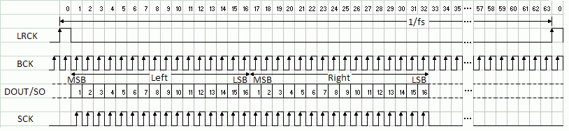
To move the data off the ADC and into the nvSRAM all that is needed is a SPI SCLK signal that is synchronized to I2S BCK and to route the ADC DOUT signal on to the SPI SO (CPLD SO is connected to nvSRAM SI line). The SPI SCLK also needs to be gated, so as to only generate 32 pulses during the write cycle (no need filling the nvSRAM with meaningless data during the other 32 cycles of the 64 cycle frame. Making the necessary changes, we have the waveforms for the ADC to nvSRAM process. (Note the nvSRAM CS signal remains low throughout the whole data acquisition burst, from the nvSRAM configuration burst, through the ADC data bursts).
I2S/SPI Timing for the DSP format and nvSRAM write
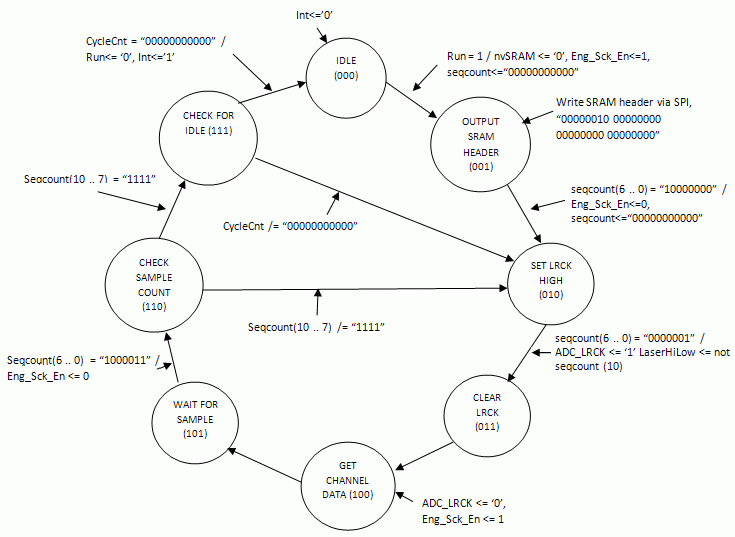
With an understanding of the interfaces between the various parts of the design, the next step is to create a State Diagram. The State Diagram describes the various states, the actions within the states and the transitions between states.
Acquisition Engine State Diagram
OK, it looks like all of the logic is well defined and we have a good understanding of where the data goes. So now it is time to work through the implementation of the VHDL coding. In working through this problem, one theme that seemed to show up consistently for me was that much of the timing seemed to be related to powers of two. The master clock is 8 MHz, ADC BCK is 2 MHz, ADC LRCK is 1/64 of BCK or 31.25 KHz, the LaserHiLow signal is 1/16 the ADC LRCK (1.935 KHz), and so on. I thought that these powers of two patterns called out for simple counters, which could be masked with other signals to create the necessary signals to drive this design. I envisioned a design based on two counters, one to drive an individual Laser cycle (seqCount) and another to run multiples of the Laser cycle (CycleCnt). The range of each counter is from 0 to 2047, or 11 bits each. The base rate of the seqCount would be 4 MHz (or master clock / 2).
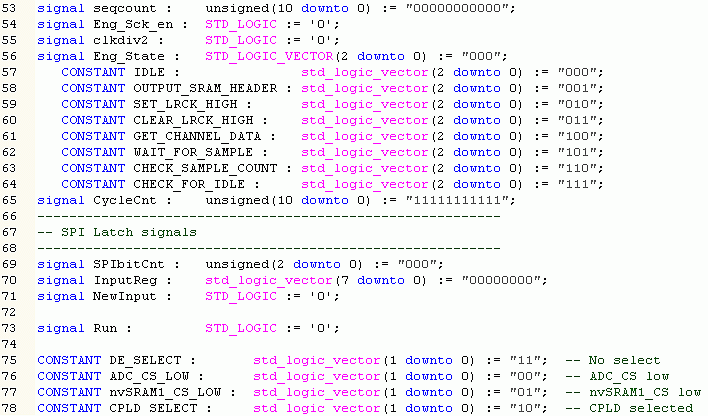
With this information, we can work through the necessary signals that will be required in our design. Shown below are the internal signals that will provide some of the underlying logic of the design. Lines 53 and 65 define are two major counters, while line 55 defines the 4 MHz clock signal that will drive our seqcount counter. Eng_State is our state variable, defined on line 56 along with the constant declarations that define each of the individual states (lines 57 to 64). Lines 69 through 71 define the internal variables that will be used to provide the SPI peripheral latch (controlling Run and the upper bits of the CycleCnt counter). The signal NewInput is a flag that will be sampled in our main state machine, which announces the arrival of a new command word. The Run signal (line 73) is the signal that kicks off the data acquisition cycle, allowing the state machine to move from the IDLE step.
The remaining lines, 75 to 78, are the constant declarations for the various states of the two chip select lines, that are used to select the targets for all SPI transactions within the data acquisition engine. The constant 'DE_SELECT' or "11" to used to allow other devices to use the SPI bus, and will be used to isolate the CPLD, ADC and nvSRAM devices from the SPI bus.
Now we can move into the logical design. The first step is to divide down the master clock signal by 2. We could have taken care of this as an extra bit in length on the seqcount counter or as an separate divider. As none of the signals in the design called for timing resolution down to 4 MHz, I went with the separate counter approach (both choices would have resulted in the same CPLD register requirements, although the separate divider approach may simplify readability and also some of the counter test conditions) . The following is the VHDL code for this counter.
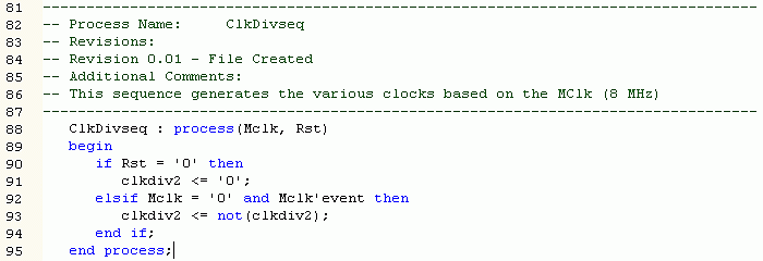
The code for this process is quite simple. If the part is in reset (line 90, Rst = '0'), the output signal (clkdiv2) is held at logic low. If the reset is not asserted, then on each falling edge of the Mclk signal, the output signal is toggled (clocked to the opposite logic state). This produces an output clock signal that is one half the frequency of the input clock (8 MHz in, 4 MHz out).
The next step is the implementation of the SPI peripheral latch. This latch will receive an 8-bit command from the μProcessor, save the value in a temporary register and signal the main state machine of an incoming command. The following is the VHDL code for this SPI latch.
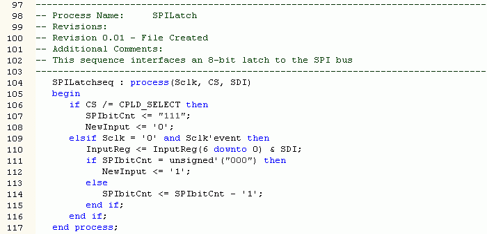
The code for this process is just a little more complex, but still pretty easy grasp. If the SPI Latch is unaddressed (line 106, CS /= CPLD_SELECT, '/=' reads as 'Not Equal to'), the SPI bit counter (SPIbitCnt) is initialized to "111" (or 7) and the New input flag (NewInput) is cleared (lines 107 & 108). If the SPI Latch is addressed, then on each falling edge of the Sclk signal (SPI clock), the SDI input is shifted into the LSB of the temporary register (line 110). Lines 111 through 115 are used to count down the SPI bit counter (if not zero) and to raise the NewInput flag if the SPI bit counter is zero.
The next step in the process is to code the state machine that will handle the collection of ADC data and the routing of the data to the nvSRAM. As this section is a little more complex, let's break it down a bit. First, let's look at the reset and clocking aspects of the main state machine.
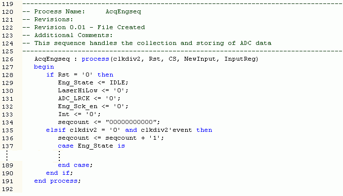 On Upon reset, the state is set to IDLE. In addition, the Laser output is set to low power, the ADC left/right clock is initialized, the internal SPI clock is squelched, the done interrupt is cleared and the seqcount is cleared. As long as reset is held, the initializations are held. Once reset is released, each falling edge of the mclk/2 signal, the sequence clock is incremented and the Eng_State case is executed. This establishes the main timing event for the Eng_State state machine. Now let's break down each state within Eng_State case.
The first state is the IDLE state. The Int output is cleared within the state to finish off the interrupt pulse started at the end of a burst. Lines 141 to 144 handle new data from the SPI Latch. If the NewIput flag has been raised, this state copies the new SPI command from the temp register (InputReg) into the Run and upper bits of the CycleCnt variables. If the Run flag was set, we kick off the burst processing by advancing the Eng_State into the OUTPUT_SRAM_HEADER state and enable the internal SPI clock (via Eng_Sck_En)

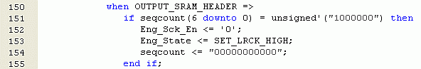
The OUTPUT_SRAM_HEADER state simply holds state until seqcount reaches a count of "1000000". Once the count is reached, the internal SPI clock is disabled, the seqcount is reset and the Eng_State is advanced to the SET_LRCK_HIGH state. All of the SPI clock and data pulses are created below by sequential logic (shown later).
The SET_LRCK_HIGH state waits for seqcount to advance to "0000001" (masking upper bits), prior to asserting the ADC Left/Right signal. This state also manages the High/Low current setting for the laser diode (bit 10 of seqcount) and advances the Eng_State to next state. This state is entered as the first step in a new burst, or as the continuation of an on going burst (within the same group of 16 samples of a complete Laser diode cycle).
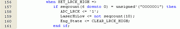
The CLEAR_LRCK_HIGH state is actually mislabeled, as this state only provides a single 4 MHz clock delay prior to actually clearing the ADC Left/Right signal. All that this state does is advance the Eng_State to the next state.
![]()
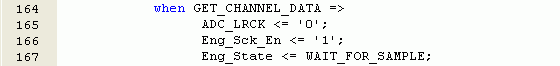
The GET_CHANNEL_DATA state clears the ADC Left/Right signal, enables the generation of the internal SPI Sck signal and advances the Eng_State to the next state. This fully conditions the logic to both clock data from the ADC and into the nvSRAM. All of the ADC and SPI clock and data pulses are created below by sequential logic (shown later).
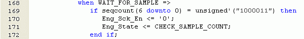
The WAIT_FOR_SAMPLE state simply holds state until seqcount reaches a count of "1000011". Once the count is reached, the internal SPI clock is disabled and the Eng_State is advanced to the CHECK_SAMPLE_COUNT state. This period represents the collection and saving of 32 bits data (from ADC to nvSRAM).
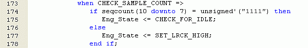
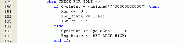
The CHECK_SAMPLE_COUNT state counts the number of ADC samples for a given Laser diode cycle. By testing bits 10 to 7 of the seqcount, it is possible to determine if a Laser cycle is complete ("1111"). If the cycle is done, the state machine advances to determine if the requested number of laser cycles have been run (CHECK_FOR_IDLE). If the laser cycle is not complete, the state machine loops back to start the next ADC sample (SET_LRCK_HIGH).
The CHECK_FOR_IDLE state determines if CycleCnt has been decremented to zero, i.e. done. If so, the Run flag is cleared, an interrupt is raised and the state machine is sent back to the IDLE state. If the CycleCnt is not zero, it is decremented and state machine is set back to start the next Laser cycle (SET_LRCK_HIGH).
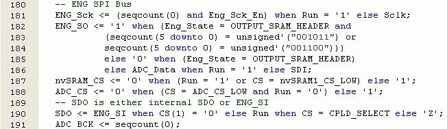
With the AcqEngseq process complete, all that remains is the sequential logic that completes the generation of some of the output signals. As mentioned earlier, the Eng_Sck_En signal is used to enable the internal SPI Sck signal. Line 181 shows that the internal SPI Sck signal (ENG_Sck) is either the logical AND of the LSB of seqcount (2 MHz) and the Eng_Sck_En signal, when 'Run' is '1'. Otherwise the Eng_Sck output is a pass through of the external SPI Sck input (Sclk).
The internal SPI SO signal (ENG_SO) is used to send data to the nvSRAM SI line. There are three different intervals when this signal is driven. First, during the OUTPUT_SRAM_HEADER state, this line is either driven high or low, based on the current value of seqcount. The value is driven low most of this time, except when the lower 6 bits of seqcount is equal to "001011" or "001100" (lines 182-185). This produces a single high going pluse on the nvSRAM SI line, during the data window of the 7th bit of the nvSRAM write preamble. Otherwise, during the rest of the 'Run' interval, the ENG_SO is driven with the current value of the ADC_Data input, or at all other times, it is driven as a pass through of the external SPI SDI input (line 186).
Lines 187 and 188 show the logic for the nvSRAM_CS and ADC_CS. The nvSRAM is selected when 'Run' is active or when the CS lines are set to "01". The ADC_CS is only used by the μProcessor and is driven low (active) when 'Run' is low and the CS lines are set to "00".
The external SPI SDO output is coded to be either the pass through of the internal SPI SI line while nvSRAM is selected (used for reading the captured data), or a status read of the 'Run' flag while the CS lines are equal to "10" (line 190). Otherwise the line is tri-stated so that other SPI devices can drive this line (when selected).
The remaining statement (line 191), causes the ADC_BCK signal to be driven with the LSB of the seqcount (2 MHz).
Whew, I think that I have made it (finally) to a good stopping place. The VHDL code is done, but we should make sure that it does what we intended. Let's leave that for next time. In part three of this article, I will presented the completed VHDL code (it mostly here, just broken up into digestible pieces), along with a testbench and some timing traces.
Until later,
Gene


- Comments
- Write a Comment Select to add a comment
To post reply to a comment, click on the 'reply' button attached to each comment. To post a new comment (not a reply to a comment) check out the 'Write a Comment' tab at the top of the comments.
Please login (on the right) if you already have an account on this platform.
Otherwise, please use this form to register (free) an join one of the largest online community for Electrical/Embedded/DSP/FPGA/ML engineers:


