


VHDL tutorial - A practical example - part 3 - VHDL testbench
In part 1 of this series we focused on the hardware design, including some of the VHDL definitions of the I/O characteristics of the CPLD part. In part 2, we described the VHDL logic of the CPLD for this design. In part 3, we will show the entire VHDL design and the associated tests used to prove that we have, in fact, designed what we started out to design.
Quick Links
- Part 1: VHDL tutorial
- Part 2: part 2 - Testbench
- Part 3: combining clocked and sequential logic
- Part 4: Creating a hierarchical design
- Part 5: A practical example - part 1 - Hardware
- Part 6: A practical example - part 2 - VHDL coding
- Part 7: A practical example - part 3 - VHDL testbench
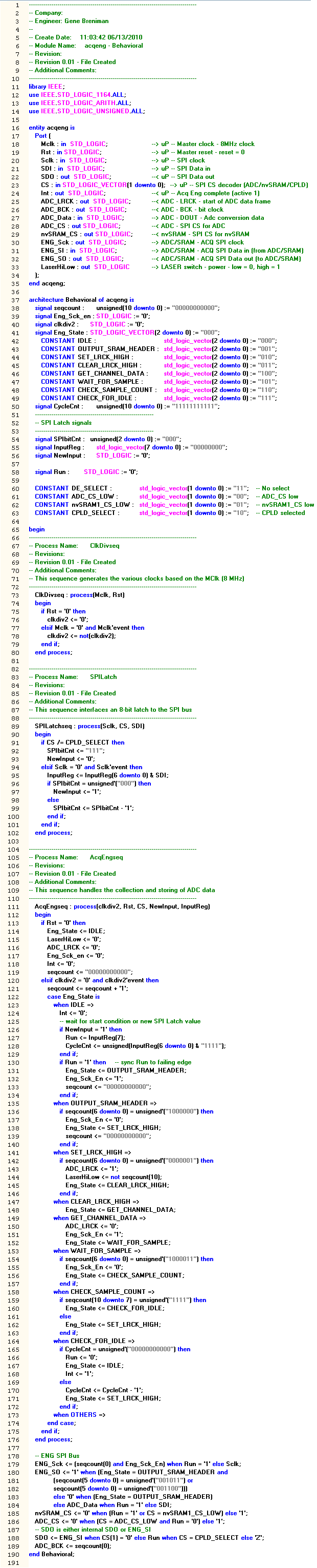
First, let's pull all of the pieces of the prior design together into a single listing. This gives us a great overview of the design and helps us to layout a testing stratagy. Here is the entire design for our data acquisition engine:
From the above code, the Xilinx ISE environment makes is simple to build the basic framework for the testbench code. To start the process, select "New Source" from the menu items under "Project". This launches the "New Source Wizard". From within the Wizard select "VHDL Test Bench" and enter the name of the new module (click 'Next' to continue). The "New Source Wizard" then allows you to select a source to associate to the new source (in this case 'acpeng' from the above VHDL code), then click on 'Next'. The Wizard then creates the necessary framework for a test bench module (see below).
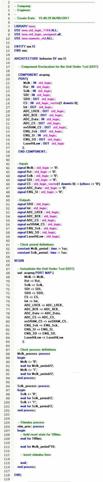
The framework above includes much of the code necessary for our test bench. It includes a component declaration section (lines 19-38), Input signal declarations and initializations (lines 41-48), Output declarations (lines 50-59) and the test component instantiation (lines 67-85). The framework also contains some canned processes for our two clock (Mclk - lines 87-94 and Sclk - lines 96-102, plus defines for clock rates - lines 62-63) and a stub version of a stimulus process (stim_proc:process - lines 105-118), which will be used to create the necessary stimulus statements to thoroughly test our design.
This framework gives us a good starting point, from which to build our complete test bench. I like to start my test bench design working through the fundamentals and then extending the stimulus generation until we have adequately exercised our design. My first steps are usually focused on clock generation. To this end, we will need to tweak some of the constants to match our target clock rates, as well as some minor changes so that we can suppress the SPI clock (Sclk) to times when we are transmitting or receiving data from SPI devices.
![]()
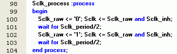
This is simple enough. The above statements change the Master clock (Mclk) and SPI clock (Sclk) to their respective rates (8 MHz and 10 MHz). Now we need to do a little modification to the SPI clock generation logic. First we need to create two signals to assist in the gating logic. The first signal, Sclk_inh, is used to enable and disable the clock signal. The second signal, Sclk_raw, is a replacement clock signal. We will be generating a gated clock signal with Sclk_raw which will be assigned to our Sclk input to our UUT (unit under test).
![]()
With the new signals defined, we can now modify the logic within our Sclk_process. In this process we will build a continous clock signal with Sclk_raw which is toggled each one-half of the Sclk_period, generating a free running 10 MHz clock. Along side of this clock generation sequence, we are creating the Sclk input by ANDing our Sclk_raw signal with a Sclk_inh signal. In this way, whenever Sclk_inh is set to '1', Sclk will be switching at 10 MHz, otherwise it will be held at '0'. We will use the Sclk_inh signal within our stim_proc process to clock SPI data in and out of our device.
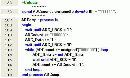
Now we need to create a process to generate simulated ADC data for our design. For this task we need a a counter to keep track of the data to be sent from our ADC simulation (ADCcount). Next we need to create a process to handle the generation of the ADC_Data line. In the process, we wait for a rising edge of the ADC_LRCK (ADC left/right clock - line 109). We use this rising edge to initialize both our ADCcount signal to the countdown value for the ADC data generation sequence (32 or "10000" in binary on line 110) and ADC_Data to '1' (line 111). We then wait for the falling edge of the ADC_LRCK signal (line 112). From there we enter a loop where we will generate a simple toggling of the ADC_Data line for our simulation (line 114). With the ADC_Data signal set, we wait for the falling edge of ADC_BCK to pace us through to the next loop (line 115). On line 116 we decrement the ADCcount value, which is tested on line 113 to determine when we have generated enough data to simulate the response of our ADC to the sequencing of the ADC_LRCK and ADC_BCK signals (you can refer back to the I2S/SPI Timing for the DSP format and nvSRAM write diagram from part 2 of this article to review the desired ADC sequence).
OK, now we need to connect all the pieces together and start to make something happen, but first, let's have a plan of attack on how to test the device. I like to start any test with a reset pulse (from high to low, followed by a return to high) and a short delay (giving us a chance to see that our main state machine - Eng_State holds in the idle state until commanded). Next we should send a SPI command to set the sample size and start the collection sequence. The rest is just waiting around until the collection burst is run. This is about all that is needed to verify the basic functionality of the device. Sure, we could add additional test to exercise all of the sample size counts (from 1 to 127), but for the time being this should be sufficient.
So, running through this quickly, line 124-157 replace the old body of the stim_proc process. As planned, we have a short reset and hold sequence (lines 124-130) and a SPI command sequence to set the sample count to one and to set the 'Run' flag (lines 132-157).
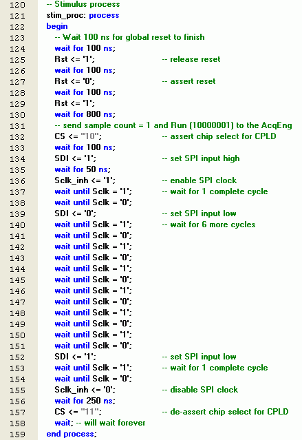
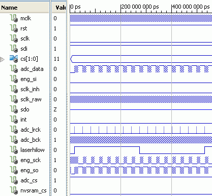
Now we can start looking at the simulation data. Running the simulation and capturing the first 2.5us, we can examine the effects of the reset pulse and the SPI command.
Let's start by examining our two free running clock signals (mclk and sclk_raw) to see if they have been generated correctly. For mclk, we can see that the signal completes 4 cycles in the first 500ns which give us a period of 500ns/4, or 125ns, giving us a frequency of 8 MHz. Good, so far we got one right. For sclk_raw, we can see that the signal completes 5 cycles in the first 500 ns which gives us a period of 500ns/5, of 100ns, giving us a frequency of 10 MHz. OK, two-for-two. Looking at the sclk signal, which is the logic AND of sclk_raw and sclk_inh, we can see that during the first 1000ns of the traces, that sclk is constant low. For now, this is what we want.
Now, let's look at how the design is effected by the reset line. In the tracings above, the reset signal starts out asserted (low), 100ns later it is released, re-asserted another 100ns later and then final released. Looking over the first 500ns, none of the traces (other than mclk and sclk_raw) are changing. This show us two things, first that reset had no real effect, there was no difference between our power up state and our reset state. It also shows that the adc_bck signal (which is the LSB of seqcount, is held low during reset). Once reset is released and two mclk cycles are completed, adc_bck begins to toggle (at a 2MHz rate).
OK, now to get things moving, we need to send a SPI command to the device, with the 'RUN' bit set, in order to start an acquisition burst. To do this, we need to select the part (CS = '10') and provide the proper data and clock sequences (Note: as the CS line is set to "10", the SDO line transitions from tri-state to Low, which is the current state of the Run flag). So, at 1.1us (800ns after the reset line was releases, lines 130-132 of our testbench) the device is selected. Then 100ns later, the SPI data line (sdi) is set high. This will be the MSB of the SPI command, or our RUN bit. After 50ns the sclk_inh signal is raised to '1', enabling the generation of Sclk pulses (8 pulses from 1.3 to 2.05us). From here, the testbench will be using edges of the sclk, so we can synchronize the SPI data line changes to the sclk. After the Sclk signal has gone high then low (lines 137-138), we clear the SDI signal, preparing to send six zeros to the SPI peripheral latch (the high bits of CycleCnt). The testbench then waits through six Sclk cycles (lines 140-151, latching in the high bits of CycleCnt). After the six Sclk cycles, SDI is driven to '1' to set the low bit of the CycleCnt register. Now, we wait one more Sclk pulse and then clear the sclk_inh line (lines 153-155), cutting of the Sclk pulse generation. To finish off the SPI write sequence, we wait 250ns and re-assert the CS lines to 'no select' state, or '11' (lines 156-157 @ 2.3 us).
Looking over the traces so far, there are a couple of things to note: 1) clock pulses on the Sclk line are being passed through the device to the Eng_Sck line (no problem here as both ADC_CS and nvSRAM_CS are held high), 2) all data on the SDI line is being passed through to the Eng_So line. Neither of these are real issues. The VHDL code could have suppressed the Eng_Sck and Eng_So signals during communications to the SPI peripheral latch within the device, but it would have added complexity to the design and may have increased the use of resources in the CPLD (it is always nice to have a few spare resources in case you need to make changes in the future). Another note worthy thing is occurring right before we are entering the 'no select' state on the CS lines, at 2.25us the SDO line goes high (right before it goes back into tri-state). While the device is in the internal SPI peripheral latch state (CS = '10'), the SDO line is constantly driven with the Run flag state. As we had just finished sending a Run command to the part, we are seeing the effect of that command, which is now causing the SDO line to go high. This is showing us that the device has in fact recognized our command, and is preparing to begin a data acquisition cycle.
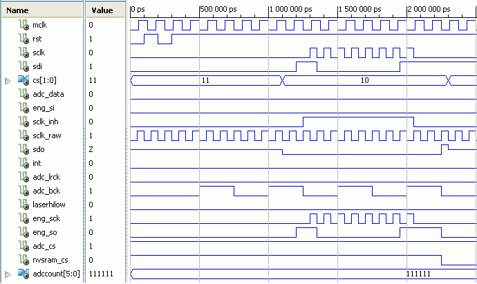
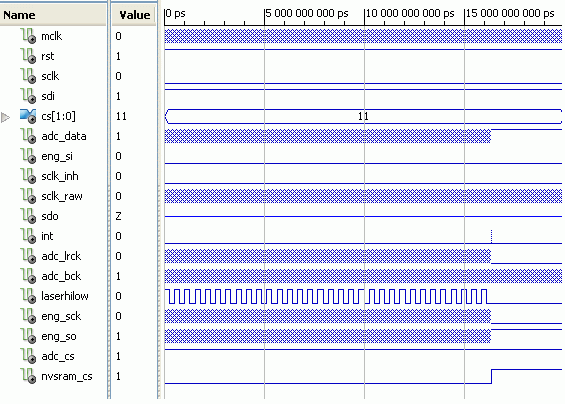
At this point, the testbench code is in a 'wait forever' stage, waiting for the device to finish an acquisition sequence. So let's look further in time and see if the device is getting it done correctly. Now let's zoom out a little further and examine the writing of the 'header' to the nvSRAM chip.
The 'header' is nothing more than the initial portion of the Burst mode write sequence for our nvSRAM device. The sequence is an 8-bit write opcode ('00000010'b), followed by a right justified, 24-bit address field (7-zeros, followed by the 17-bit nvSRAM start address of zero). Examining the above traces, starting at ~2.25us, we see the nvSRAM_CS line going into the select state ('0'). This will be the case throughout the rest of the acquisition sequence. Shortly after nvSRAM_CS goes low we see 32 pulses of the Eng_Sck signal, along with the nvSRAM data of six zeros, a one and 19 more zeros (measured at the rising edge of Eng_Sck).
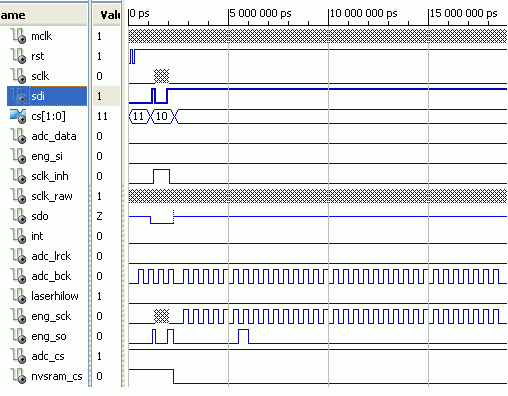
Now let's look at the first ADC sample sequence. This is where the ADC is strobed (ADC_LRCK), followed by a series of serial bit clocks (ADC_BCK).
Zooming in for a little more detail on the ADC signals (below), we can see the beginning of the ADC cycle. On the falling edge of ADC_BCK, ADC_LRCK goes high and then returns low on the next falling edge of ADC_BCK. At this point the first bit of the ADC data (MSB of the Left channel) is present on the Eng_So line (in this case '0'). In order to clock the ADC data bit into the nvSRAM, it must be stable for the rising edge of the Eng_Sck. So far, it looks like everything is moving along correctly. In the above image, we can see the toggling pattern of '1' and '0' (as generated by lines 113-117 inside of our ADCcmp process of the testbench). There are a total of 32-bits (16 - '0'/'1' sequences) on Eng_So and the ADC_data lines, along with 32 cycles of the Eng_Sck clock (writing the two ADC values as four byte writes to the nvSRAM). The ADC_BCK continues to clock through the ADC frame as detailed in the specification sheet for the ADC part.
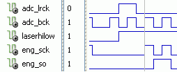
With the ADC cycle verified, we zoom out again and look at a full Laser diode cycle (below). There are 16 ADC cycles (counting the ADC_LRCK pulses) within the full cycle of the LaserHiLow signal.
With Laser diode cycle verified, we zoom out yet again and look at a full acquisition cycle (below). There are 32 Laser diode cycles (counting the LaserHiLow pulses) within the full acquisition cycle. At the end of the data acquisition cycle we can see the short high pulse of the Int (interrupt) signal, which informs the μProcessor that the requested cycle is complete.
That pretty much completes the verification phase. It looks like everything worked OK. Well, there was a little glitch in the process that I glassed over before. In the nvSRAM header testing I noticed a small error with the placement of the high going pulse on the Eng_SO line. The simulation traces were corrected, but now I need to correct the VHDL source for the device. So here is the change:
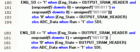
Lines 180-184 at the top have been replaced by lines 180-183 at the bottom. The effect of the change is to move the '1' during the nvSRAM header sequence back in time a little bit. In the upper sequence the ENG_SO line is high from seqcount "001011" to "001100". In the lower sequence the ENG_SO line is high from "001100" to "001101". The coding on the lower sequence is simpler in that we can ignore the LSB of seqcount and trigger our change on bits 4 to 1 (ignoring bit 0).
Whew, I think that I have made it (finally) to the end. We have taken an idea or specification through the phases of hardware design, VHDL coding and finally testing. Once again I have proven to myself (and hopefully to you) the importance of testing. Mistakes are hiding out there all you have to do is find them and fix them.
Until later,
Gene


- Comments
- Write a Comment Select to add a comment

Gene, I cannot thank you enough for you great effort. To share something that is beyond the accademical scope gives the true insight into how I can turn "bare" knowledge into useful products. Much appreciated!

Hi Gene, did you know that this article of yours is now at more than 70,000 pageviews?
You've helped lots of people with it over the years.
hi can you post the corrected one?
I'm new to this field and trying to make a VHDL code for my project thesis. I'm trying to make a code for SPI core to ARINC 429 interface which I have to simulate in Model sim. Please Gene help me.
I'm from sensor field and don't know much about coding in VHDL. I have learnt VHDL but still not very good in writing the code. I'm very grateful if u can help me in writing the code. Thanks in advance.
To post reply to a comment, click on the 'reply' button attached to each comment. To post a new comment (not a reply to a comment) check out the 'Write a Comment' tab at the top of the comments.
Please login (on the right) if you already have an account on this platform.
Otherwise, please use this form to register (free) an join one of the largest online community for Electrical/Embedded/DSP/FPGA/ML engineers:


