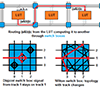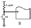





Jon Elson wrote:> Al wrote: > >> Hi to everyone, I'm trying to generate a 5-10 ns pulse width out of an >> edge, without the use of any clock, just with internal delays. >> Unfortunately I can imagine how much this delay will depend on >> temperature and voltage and how much the width will be affected, but >> still I have some margins (anyway everything will be tested in a >> thermal chamber to verify functionalities). >> So far I developed a sort of a "ripple-counter" with an auto-reset for >> each FF (Q(0) will asynchronously reset Q(0)) so that I can start an >> internal oscillation (a clock!). >> After that a normal counter can be realized on the basis of this >> clock, allowing to build a pulse. Once the pulse is over a reset is >> generated to stop asynchronously all the FFs. > > > I needed a delay to advance an address counter after a bus strobe > ended. It was for a CPLD on a small plug-in board, and there was > no other need for a clock on the board. So, I routed the signal out > one pin, through a 1.5 K Ohm resistor, and into another pin. The > input capacitance of the pin became the C of the RC time constant. > This has worked well in the application. > > In your case, taking the signal through a similar external delay, and then > bringing it back in to an AND2B1 for a pulse only on the rising edge, > or an XOR if you want pulses on both edges should do what you want. > Adjust the resistor value to get the desired time delay. > > It may also be possible to route to an unbonded IO pad with weak drive > and get a fair amount of delay, easily 5 ns, but probably not 10. > > JonAl mentioned he wanted to avoid a PCB respin, but he could certainly look for spare IO pin(s), and make use of the pin path delays. It may even become probe-able ? -jg
run a counter without a clock
Started by ●November 24, 2006
Reply by ●November 27, 20062006-11-27
Reply by ●November 28, 20062006-11-28
Jim Granville wrote:>> I needed a delay to advance an address counter after a bus strobe >> ended. It was for a CPLD on a small plug-in board, and there was >> no other need for a clock on the board. So, I routed the signal out >> one pin, through a 1.5 K Ohm resistor, and into another pin. The >> input capacitance of the pin became the C of the RC time constant. >> This has worked well in the application. >> >> In your case, taking the signal through a similar external delay, and >> then >> bringing it back in to an AND2B1 for a pulse only on the rising edge, >> or an XOR if you want pulses on both edges should do what you want. >> Adjust the resistor value to get the desired time delay. >> >> It may also be possible to route to an unbonded IO pad with weak drive >> and get a fair amount of delay, easily 5 ns, but probably not 10. >> >> Jon > > > Al mentioned he wanted to avoid a PCB respin, but he could > certainly look for spare IO pin(s), and make use of the pin path delays. > It may even become probe-able ? > > -jg >Hi guys, well, as Jim said I wouln't like to respin the pcb, but still the IO delay could be used because there are some close pins which are not used and can be easily shorted, but unfortunately I need to instantiate a lot of these delays. So either I implement a free running counter with this delay to generate an internal clock and then do all the things I need, or I simply try to count on the internal routing delay, which is quite ok on post-layout sim, but still have to try it on the hardware! I will post my results next week, when I will do some tests. Thanks to all Al -- Alessandro Basili CERN, PH/UGC Hardware Designer
Reply by ●November 28, 20062006-11-28
Al schrieb:> Jim Granville wrote: > >> I needed a delay to advance an address counter after a bus strobe > >> ended. It was for a CPLD on a small plug-in board, and there was > >> no other need for a clock on the board. So, I routed the signal out > >> one pin, through a 1.5 K Ohm resistor, and into another pin. The > >> input capacitance of the pin became the C of the RC time constant. > >> This has worked well in the application. > >> > >> In your case, taking the signal through a similar external delay, and > >> then > >> bringing it back in to an AND2B1 for a pulse only on the rising edge, > >> or an XOR if you want pulses on both edges should do what you want. > >> Adjust the resistor value to get the desired time delay. > >> > >> It may also be possible to route to an unbonded IO pad with weak drive > >> and get a fair amount of delay, easily 5 ns, but probably not 10. > >> > >> Jon > > > > > > Al mentioned he wanted to avoid a PCB respin, but he could > > certainly look for spare IO pin(s), and make use of the pin path delays. > > It may even become probe-able ? > > > > -jg > > > > Hi guys, well, as Jim said I wouln't like to respin the pcb, but still > the IO delay could be used because there are some close pins which are > not used and can be easily shorted, but unfortunately I need to > instantiate a lot of these delays. So either I implement a free running > counter with this delay to generate an internal clock and then do all > the things I need, or I simply try to count on the internal routing > delay, which is quite ok on post-layout sim, but still have to try it on > the hardware! > I will post my results next week, when I will do some tests. > > Thanks to all > > Al > -- > Alessandro Basili > CERN, PH/UGC > Hardware Designerburied ring oscillator tends to run at rather high frequencies, so you may use a single unused IO pin as pin-pad-oscillator (just route pad in over inverter back to pad, may have to add always true tristate control to avoid synthesis issues) this will usually oscillate at lower frequencies, and in most cases will have constant routing without special tricks to lock the instances Antti
Reply by ●November 28, 20062006-11-28
Jim Granville wrote:> Depending on what exactly you are using this for, you could also look > at 'margining' it - generate a tapped delay, and use a faster tap for > your delay, and check the longer one was still (just) OK, which > means the faster one was OK with margin.Sorry Jim, I didn't understand correctly what do you mean by that.> > Or, even build a calibrate phase into the tap selection. >Don't understand this either> On the 'going faster' sense, the FPGAs tend to self-compensate : A > fast process device will give, and tolerate, faster delays, and a > hot device will give, and need, longer delays. > Generally the big problems come when the delays run into the > next clock edge :) >Could you give me some reference about what you said or simply explain this to me in a more detailed way? You can contact me directly if you think this is not the place to go in details. Thanks a lot Al -- Alessandro Basili CERN, PH/UGC Hardware Designer
Reply by ●November 28, 20062006-11-28
"Jim Granville" <no.spam@designtools.maps.co.nz> wrote in message news:456b5eea$1@clear.net.nz...> > Al mentioned he wanted to avoid a PCB respin, but he could > certainly look for spare IO pin(s), and make use of the pin path delays. > It may even become probe-able ? >Guys, I used an unbonded IOB to get delay once. Drove a signal to its unbonded pad and got the signal back through the IOB delay thing on the same unbonded IOB. Who knows what the delay would be from device to device, but it was good enough to deglitch a 19MHz clock. If you do this, you need to turn of the DRC in the bitgen part of the tool flow. HTH, Syms.
Reply by ●November 28, 20062006-11-28
Symon wrote:> "Jim Granville" <no.spam@designtools.maps.co.nz> wrote in message > news:456b5eea$1@clear.net.nz... > >>Al mentioned he wanted to avoid a PCB respin, but he could >>certainly look for spare IO pin(s), and make use of the pin path delays. >>It may even become probe-able ? >> > > Guys, > I used an unbonded IOB to get delay once. Drove a signal to its unbonded pad > and got the signal back through the IOB delay thing on the same unbonded > IOB. Who knows what the delay would be from device to device, but it was > good enough to deglitch a 19MHz clock. If you do this, you need to turn of > the DRC in the bitgen part of the tool flow. > HTH, Syms. > >What is the DRC in the bitgen? Thanks Al -- Alessandro Basili CERN, PH/UGC Hardware Designer
Reply by ●November 28, 20062006-11-28
"Al" <alessandro.basili@cern.ch> wrote in message news:ekhe85$snq$1@cernne03.cern.ch...> > What is the DRC in the bitgen? > Thanks >Al, http://catb.org/esr/faqs/smart-questions.html HTH, Syms.
Reply by ●November 28, 20062006-11-28
Al wrote:> Jim Granville wrote: > >> Depending on what exactly you are using this for, you could also look >> at 'margining' it - generate a tapped delay, and use a faster tap for >> your delay, and check the longer one was still (just) OK, which >> means the faster one was OK with margin. > > > Sorry Jim, I didn't understand correctly what do you mean by that.It depends on just what you are trying to do - it sounds like you have some sort of centering issue ? The idea above means to create a number of delays, and then use one, but check with another - so you can at least flag a failure. The simplest delay schemes have no error flags>> >> Or, even build a calibrate phase into the tap selection. >> > Don't understand this eitherTo do this, you need again a tapped delay line, only now you add a CAL phase - again, system dependant, but often you have a pulse/chipselect of known width, and that is used to sample/latch the Chip delay line, and store the result. That number then selects a tap to use in the desired delay. Rather more complex than a simple IO pin delay, but it self-tracks. Downside is you need a CAL pass before it is valid. -jg