


DDC in FPGA with high speed ADC
Hi all
I'm going to work with high speed ADC in my upcoming project. I'm having 4 ADC channels with 3.2GHz sampling rate interfaced with FPGA. I'm getting 40 samples at every 80MHz clock rate (80*40=3200MHz). My band of interest is 750MHz to 1250MHz. I'm little bit confused in DDC with this high speed data rate. In FPGA we can't operate at 3.2GHz. I want to carry my band of interest with 800MHz sampling rate in complex domain. Can anyone suggest me some ideas for DDC?
Thanks and regards
Loganathan N

Hello,
If I understand correctly you want Fs = 800MHz. You also want 750MHz to 1250MHz centered in base-band so Fc = 1000MHz. That gives a complex base band +-250MHz. Yes?
I would first do a Fs/4 complex rotation followed by 1 half-band decimating filter. This gets you down to Fs = 1600MHz. Your base-band now has a complex signal that is centered at 200MHz.
Now you can do a Fs/8 rotation followed by another half-band. Now Fs = 800MHz and your signal is centered at DC.
Of course the implementation is massively poly-phase.
Cheers,
Mark Napier

Hi Mark,
I'm working on something very similar as the OP. Totally understand the part about using a half-band filter, doing that too (as a Xilinx polyphase filter), but wanted to clarify something.
Is the Fs/4 complex rotation you're talking about just a way to convert the real samples into complex ones (quadrature conversion), or is it something else that I'm missing? And why is it done a second time?
Hello,
This is a down-conversion process. The center frequency Fc is 1000MHz sampled at Fs = 3200MHz. The BW of interest is 500MHz wide.
So 1st do a complex rotate by Fs/4 = 800MHz. Yes this is a quadrature conversion. The in-phase multipliers are 1,0,-1,0 or cos(0), cos(pi/2), cos(pi), cos(3pi/2). The quadrature multipliers are 0, 1, 0, -1 or sin(0), sin(pi/2), sin(pi), sin (3pi/2). The beauty of the Fs/4 rotation is that there are no multiplies, only commutators and inverters. So that rotates an 800MHz center frequency to DC. The max frequency of interest now at DC is 1250 - 800 = 450MHz and Fc is now at 200MHz. Design a half-band decimating filter with the roll off just beyond 450MHz.
So now the sample rate Fs = 1600MHz. Rotate by Fs/8 = 200MHz. The values for in-phase are [cos(0), cos(pi/4), cos(pi/2), cos(3pi/4), cos(1), cos(5pi/4), cos(3pi/2), cos(7pi/4)]. This shifts the 200MHz center frequency to DC. The max frequency of interest is now 250MHz. Design a half-band decimating filter with the roll off just beyond 250MHz. This gets you down to Fs = 800MHz.
In both of these stages the challenge is the data rate. The data will have to be processed in parallel to meet timing. In both of them it may be possible to arrange the data paths in some (sub)multiple of the half-band tap weights and rotation multipliers so that processing is shared. Fred Harris' book on multi-rate processing is a good resource.
Assuming this design is done in hardware, I like to design filters that use CSDs (canonical signed digits) rather than multipliers. This uses adders rather than multipliers. In principle it uses less hardware and runs much faster than multiplier implementations and this is absolutely true in ASIC design. For FPGA's I don't know. The fabric needed for the adder trees may be more than just using the DSP slices. Really depends on the complexity of the filter.
Maybe someone else know if a DSP slice or a simple adder runs faster in an FPGA. Probably the adder. If there is any interest, Neil posted a nice intro to CSD filter design.
Best regards,
Mark Napier
Hi Mark,
your approach is the right one (rotation FS/4, Half Band, rotation Fs/8, HalfBand), I wrote a little too fast at first place (and perhaps too late!). In current FPGAs there is an insane number of hardware multipliers running at the maximum clock rate achievable, so the CSD is only used when you run out of these multipliers.
On Xilinx FPGAs actually, there is no adder tree but adder chains (transpose and systolic form FIR filters) that is included in the DSP slice.
Super Sampling Rate (SSR) architecture for the FIR is not available within System Generator so, Loganathan, will have to design it yourself.
Loganathan: Contact me at olivier.tremois@xilinx.com I'll be able to help you.

I would rather go for direct down conversion to dc by rotating by 1000MHz then apply one fractional decimator to downsample from 3200MHz to 500MHz. This is so since mixer design is not problem though will take resource compared to Fs/4 or Fs/8.The decimator architecture is far more involved and one hard fir design is better than multiple different ones.
If you have the FPGA fabric and resources to spare sure.
In ASIC design we are always trying to minimize area and power. The chip costs so much it is worth some engineering time to get to a "optimal" solution. Its really hard to beat the efficiency of decimating half-bands when they are chained together. Note that the desired final Fs is 800MHz so it naturally lends itself to this approach. I've done a few of these so I always think this way. These two filters will have a large transition band so the order needed for the FIR is quite modest. Also, the 1st rotator has every other value at 0 so there is some savings to be gained there with some work.
But yes, if there is a system generator that will spit out the working code then the brute force approach is quicker at the expense of more hardware. For a job where the FPGA is huge and time is tight then that is the right answer. For me, it is always the case that there is one more feature that needs to be shoved into that FPGA.
If you haven't guessed, I'm a very big fan of Fred Harris and also Michael Rice. Love the whole concept of doing more with less and a little trickery.
Hi Olivier,
Kindly take a look at my detailed answer & suggest me for any better way of implementation. Thanks for your interest showing on my queries.
Thanks & Regards
Loganathan N
Thanks for the detailed answer. Your suggestions are really perfect for multiplier & memory(DDS) less frequency shifting. Now I've came up with some simple logic for this DDC.
The algorithm part that I need to do is simple phase difference calculation between 4 ADC channel (Each channel operating at 3.2GHz) with my band of interest 750 to 1250MHz (500MHz BW) and I've to match the phase difference within +-8deg between all the 4 channels.
I thought to down convert my band of interest to DC & I can proceed for FFT with 512 or 1K point. With FFT I can find the frequency, power & respective phase. But to process my 500MHz band width in complex domain, surely I need more than 500MHz sampling rate. If I decimate by 4times, I'll get 800MHz sampling rate to process my band of interest. This will be sufficient for 500MHz band width. But operating the DSP48E2 slice at 800MHz will not be recommended.
Hence I've decided to carry my band width in 2 chains each of 250MHz band width(750 to 1000 and 1000 to 1250). Each band I can operate at 400MHz sampling rate. So, I need to decimate by 8 times. And my data also coming at 8 parallel arms.
Algorithm:
Initially I beat the ADC data with 875MHz(for 750 to 1000MHz band) DDS generated frequency. Respective phase offset I've applied between all 8 parallel data. This frequency shifted 8 parallel data I've given to following FIR filter with decimation function.
I've designed a Symmetric least square LPF with 50MHz Fpass, 270MHz Fstop & order of 23. This filter gives me 6dB attenuation at 125MHz. This will be sufficient for me. So, totally 24 coefficients are there with symmetric structure. For implementing efficient symmetric coefficient FIR filter, I've followed the below realization structure with decimation factor of 8.
With current 8 samples and 16 previous samples, I can directly apply to this filter. For every new 8 samples I'll get an output.
With this algorithm I need 8 multipliers for frequency shifting. As the coefficients are symmetric (N+1)/2 multiplication is sufficient. For filtering I need 12 multipliers for coefficient (Order N=23) multiplication. And for adding all the 12 multiplers output I need 3 DSP slice. Twice the above resource will take for both In phase & Quadrature Phase component.
I don't think that it might be the efficient way of implementing. If anything kindly suggest me.Thanks & Regards
Loganathan N
Mark, thank you for your detailed reply. This helped a lot, and got me looking at downconversion the right way, wouldn't have gotten there without the tip.
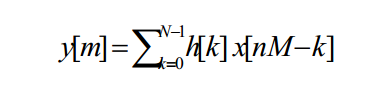
Now that I knew what to look for, I found a book that helped make this even clearer: Sample Rate Conversion for SDR (https://www.amazon.com/Sample-Conversion-Software-...), and there they show that the equation for the downconversion of a signal to baseband is
realized by multiplying the IF (or RF) signal with a rotating complex phasor. The complex samples of the rotating phasor can be from a CORDIC or ROM.
According to the Xilinx system generator DDC docs, the Xilinx DDC works exactly this way.
Hope it works out for you. I haven't used the system generator, just code in RTL (Verilog if possible). Am doing more Xilinx work now so do need to get more familiar with it.
Cheers,
Mark Napier
I think both approaches to down conversion are possible i.e to 200MHz then dc or direct to dc. A parallel mixer is not a problem.
However the downsampling filter(s) will be the challenge because the single signal stream is now divided into several parallel streams and there is inter-dependency between them. You cannot just apply same filter to each branch of signal.You will need to model the filter shared across several parallel modules before you go further.
I agree completely. The trick is the parallel design. What I use is Simulink with a custom block set. It allows you quickly try out different approaches in a fashion that closely models hardware. Once that is working then implement in RTL.
Hi Loganathan,
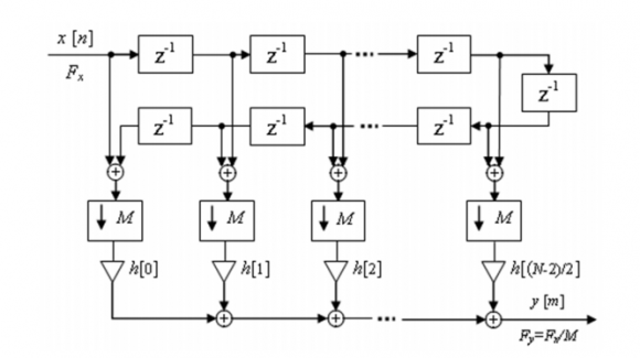
you have to implement what we call a Super Sampling Rate architecture.
So to speak, you have to process multiple samples in parallel.
What I understand from your axplanations is that you have a single channel @3200Msps.
If I refer myself to Xilinx FPGAs, you must have Kintex/Virtex class of FPGA, so with a careful design you can achieve 400MHz clock rate. In that case at each clock cycle you get 8 samples per clock per channel.
First stage you have to shift your band of interest around 0. In order to do that you need 8xDDSrunning @ 400MHz and with a phase in between them (1/8th the increment of the phase counter). You mix your 8 samples with the right sin/cos from the DDS.
Now you need to Down Convert 5/32. You can first use 2 Halfband filters to downsample by 2x2, and then a rational ratio 5/8. All these filters should be SSR filters, hence processing multiple samples at the same time:
- 8 for the first half-band
- 4 for the second half-band
- 2 for the last 5/8 downconversion filter.
Hi Oliviert,
Yes you're right, we're using Ultrascale FPGA.
At what rate I've to design my Half band filter, either at 3.2GHz or 400MHz. What do you mean by SSR Filter?.
Whether I've to use a separate Half band filter for all the 8 parallel arms with the same filter coefficients? Like x(n), x(n+8), x(n+16).. etc to the first Half band filter and x(n+1), x(n+9), x(n+17).. etc to the second half band filter.
Thanks & Regards
Loganathan


