


MyHDL FPGA Tutorial I (LED Strobe)
Last updated 05-Nov-2015
Introduction
From many perspectives the latest FPGA offerings from 'X' and 'A' are large devices - mucho programmable logic resources. Even the devices that one can get for sub \$10 are relatively large. Because of the size of these FPGAs they are implemented using an HDL. To manually configure each circuit would be a long and tedious task. It is not feasible to program an FPGA by manually defining the logic for each LUT and manually connecting the logic blocks. To implement (configure) an FPGA the use of an HDL or other high-level description tool is required. We rely on EDA software to translate the hardware descriptions to bit configurations used to program the FPGA.
Note: Yes, it is possible to program an FPGA schematically and build a hierarchy (similar to structural HDL). This is rarely used, schematic design is used for small "glue" logic or top-level stitching of the blocks together.
As mentioned, majority of FPGA designers and FPGA hobbyist will define their FPGA designs with an HDL (hardware description language). For many people doing an FPGA project, if they have been introduced to an HDL in the past, they will choose Verilog or VHDL as their HDL. They will select Verilog/VHDL because that is what they were taught. But doing so they are missing out on another excellent HDL called MyHDL. MyHDL is a Python package that allows digital hardware description in Python.
For reasons why you would want to use MyHDL see Why MyHDL . Also, the MyHDL manual is a good reference. Jan Decaluwe has done an excellent job creating and maintaining MyHDL.
The following is a tutorial using MyHDL to implement a design and run the FPGA tools generating a bit-stream for a development board. This tutorial has automated scripts to build the design for the following development boards: DSPtronics SignaX1 (SX1); Digilent Nexsys2, Atlys, Zybo; teraAsic DE2, DE0nano; XESS Xula, Xula2, CATBoard; and USBP boards. The design of the HDL is board independent, for this design all that is required is a bank of LEDs and a clock. The only board dependent constraints are the pin mappings and the clock frequency. The generation of the constraints is handled by the conversion script, creating the FPGA specific constraints and running the tools are handled via Python as well (one-stop language for this tutorial).
FPGA Development Boards
Each of the development boards used in this tutorial have medium sized FPGAs and a bank of LEDs available. The boards used ares ones I had laying around that made it easy to download the designs once the bit files were created. As mentioned, for this tutorial everything after the design entry has been automated. There is one script to create a bit file. This does require that the FPGA tools be installed and accessible (path to the tools is in your PATH so that the script can access the tools). Thanks to Guenter Dannoritzer for creating a Python script to run the Xilinx tools . The script has been expanded and modified to support additional tools.
Prerequisites
To walk through this tutorial it is presumed that the MyHDL manual has been reviewed and/or one is familiar with digital circuit design, HDL design, Python, and willing to jump in head first!
LED Control
The circuit that will be described here is a simple LED control circuit._ The module we want to define will strobe the LEDs on an FPGA development board. If you are familiar with the 80s pop-icon David Hasselhoff's Pontiac Trans Am (or the recent version of KnightRider) this might look familiar.
KnightRider stroby
To implement the design we are going to define the behavior of the circuit in MyHDL. We want to describe the behavior to strobe the LEDs back and forth at a constant rate. We will outline the main components that need to be described.
On the development boards we have a clock. This clock will usually run at some 10s of mega-hertz (MHz). On the SX1 board the main clock is 48MHz, ufo400 48MHz, the Nexsys2 50MHz, and the DE2 50MHz. The clock is the only input to our circuit. Based on this single input we will describe the behavior to create this strobe effect. The strobe will not operate at the frequency of the clock, the LEDs will shift at some rate much slower than the circuit clock. One of the components that needs to be described is a clock counter. A piece of logic that will count clock cycles and generate a pulse -much slower pulse- periodically. This will indicate when the LEDs should shift.
MyHDL Short Introduction
At this point we will take a slight detour and take a quick look at a MyHDL module. We will use a shift register as an example. Describing a shift register in MyHDL is straight-forward. We need to declare a signal of n bits. And use the shift operator. The following gives the anatomy of a MyHDL module and implements the shift register logic.
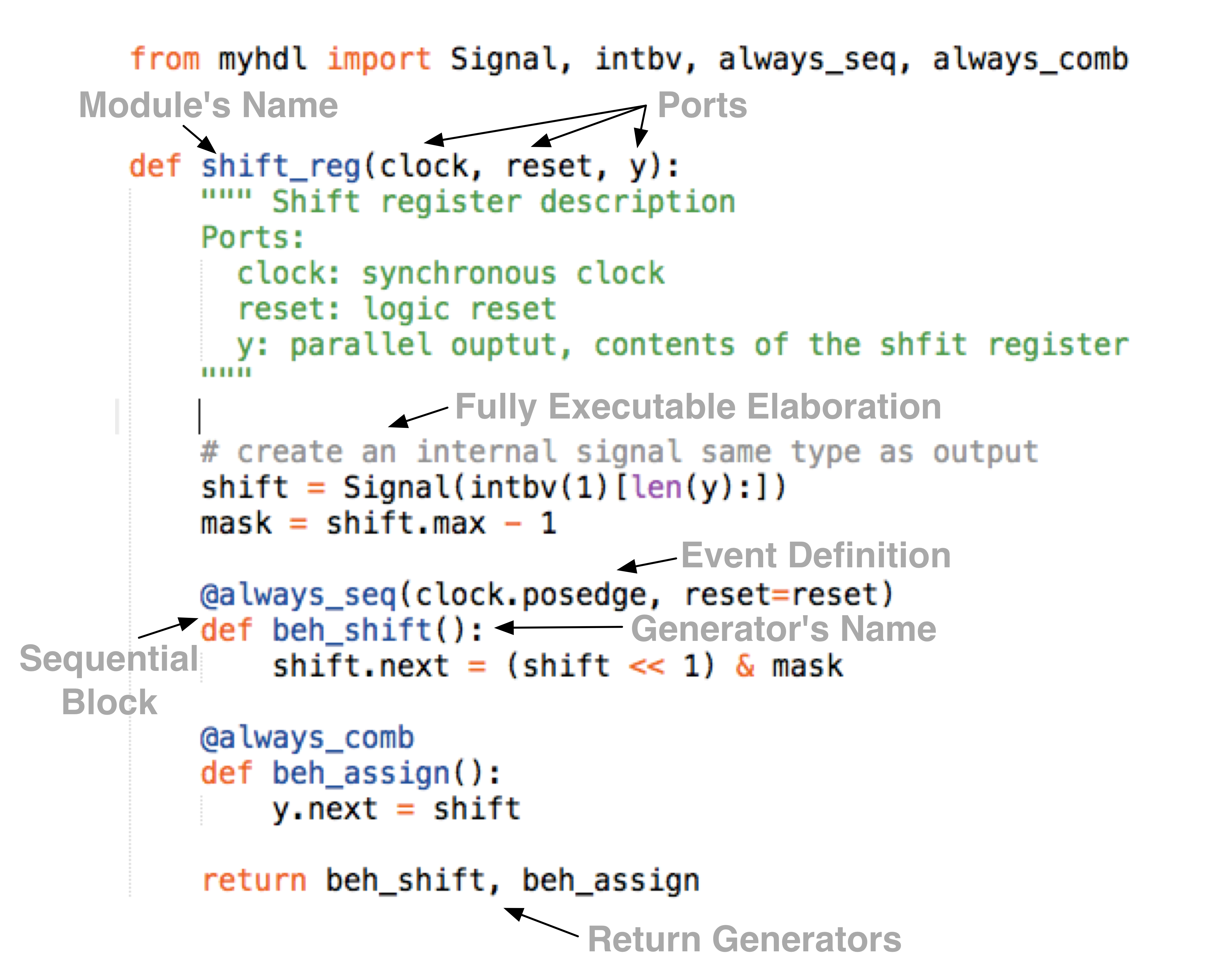
The above code snip will simply set the collection of flip-flops to 1 (0001b in the above example) and shift the 1 to the left 1 bit on each clock cycle.
I did not implement a self checking testbench in the above example but I will below for the complete example.
Back to the design example
The previous section was a short introduction to MyHDL modules, that is, what is involved to describe a hardware block using MyHDL/Python. We want to continue on with our basic design example. We are defining a digital hardware block that will "strobe" a bank of LEDs. The digital hardware will turn an LED on for a period of time and then move to the next LED. A strobe is defined as the "ON" LED moving left or right at a defined rate.
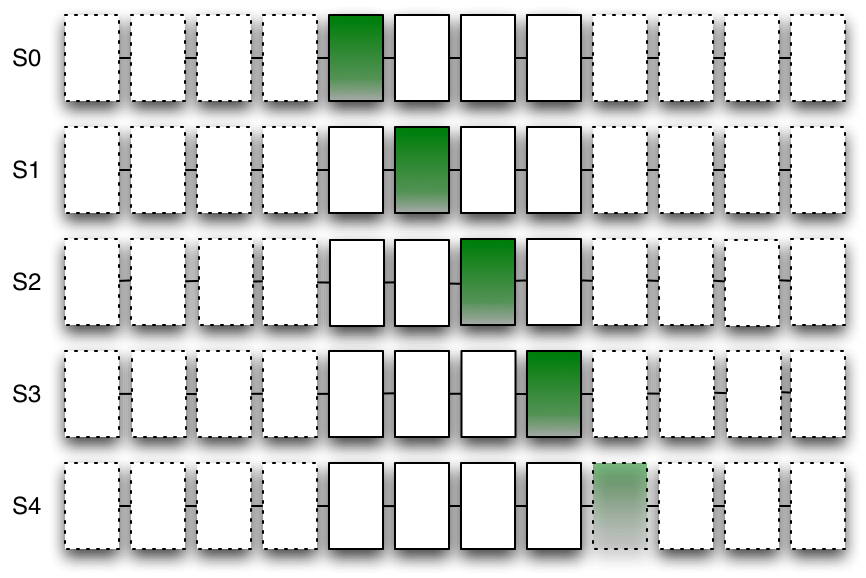
Example LED strobe
The above graphic, each line, is a snapshot in time. The on LED will move one to the left or right. When the on LED is the most left or right the direction will change. The dummy LEDs are used so no LEDs are on when the LED moves off the end (i.e. the on is a dummy bit). The number of dummies are the delay that will occur (x2) at each end. In the above example 4 dummy bits are defined and the LEDs are on for .3 seconds each. The off delay will be 2*4*.3 = 2.4 seconds on each end.
At this point we have enough description of our design to capture important design parameters.
- Frequency of the input clock
- The rate the LEDs strobe
- The number of LEDs in the LED bank (number of LEDs on the hardware development board)
- The number of dummy bits (delay on the ends)
The above defines the parameters to our module and the following is the module definition using the design parameters.
def led_stroby(
  # ~~~[Ports]~~~
  clock,                 # input: system sync clock
  led,                   # output: to IO ports drive LEDs
  reset=None,            # input: reset
  # ~~~[Parameters]~~~
  clock_frequency=48e6,  # clock frequency
  led_rate=333e-3,       # strobe change rate of 333ms
  num_dumb=4,            # The number of dummy LEDS on each side
):
From the above definition two inputs are defined: clock and reset and one LED bit-vector output. In addition to the ports, the parameters for the module. We have described the functionality requirements, ports, parameters to the design. Now lets look at testing the design.
Test
One of the big benefits of using Python/MyHDL as the HDL is that all the tools of the Python language are available for verification. We are going to define a test before we actually code up the design. The test in this tutorial is basic, verify that the logic moves the "ON" LED to the right or left. The test will monitor the LED port and verify that the LED is shifting. The following code-snip shows the generator function to verify the LED movement and configured delay.
The above will monitor for one of the LEDs to be "ON". When one of the ends is on it will determine the direction and keep track of the time (ticks) between the current led being on and the next on.
Refer to the code-listing for the complete testbench and verification code.
The code referenced is the simulation testbench. This will instantiate the design and verify that the LED is shifting back and forth. The testbench uses a generic template so that it can be used with the py.test unit test framework. The portion of the code that verifies the LED and count is wrapped in a generator, this way different tests (configurations) can utilize the same functionality. In other words, additional tests can easily be added.
Also notice, the test_random function includes constraint random
testing. Python is a full-blown modern programming language and,
essentially, is unlimited in the tools available for verification.
At this point we don't implemented any of the module functionality but provide a minimal stub to run the test.
Create the following files in your local environment:
- stroby.py (fpga25_snip3.py in the gist)
- test_stroby.py (test_stroby in the gist)
With the files created we can run the test and verify it fails.
>> py.test test_stroby
HDL
To describe our functionally we need storage elements that we will
call
led_bit_mem. We also need a counter to divide our FPGA clock
down and generate a strobe to shift. Basically, we need to describe a
counter and a shifter with some states (shift left, shift right,
change direction).
Below is the complete code listing for our behavioral model.
With the complete HDL description the tests can be rerun and the
test should now pass! In addition, the
test_stroby.py will convert
the design to Verilog. A Verilog compiler such as
Icaraus Verilog can be used to verify the converted Verilog
compiles without error.
>> iverilog led_stroby.v
FPGA tools
Now we have a couple other tasks to complete before we can download the design to the FPGA development boards.
- Convert the design to Verilog/VHDL
- Run the FPGA vendor tool chain (synthesis, PaR, bit-stream generation)
- Download the design to the FPGA development board
See the tool install
page
for more
information on installing the packages and tools. The build
process has been automated, the
test_and_build_stroby.py script
can be used to build the FPGA bit file.
>> python test_and_build_stroby.py --build --board=cat
The above command will map the correct pins and invoke the FPGA toolchain for the appropriate board. The automation has only been tested on a Linux machine. The automation does not need to be used, the converted file can be imported into the vendor toolchain.
FPGA vendor tool chain
We are not going to specifically review how to use the vendor FPGA tools in this tutorial. If you are unfamiliar with the FPGA vendor tools the following links might be useful.
The automation process creates projects for each of the toolflows. The generated projects have been saved.
Download
Downloading the design will depend on the board and software tools used. The USBP and SX1 have separate software programs to load the bit-files. The nexsys2 and DE2 can be programmed with the vendor design software. The xula boards have an easy to use Python package xstools that can be installed via pip. Refer to the development board documentation for the appropriate configuration methods.
Video Slow Blinking on UFO400
Conclusion
This was an introductory tutorial using MyHDL as the design language for FPGA implementations. Questions on this tutorial can be submitted in the comments section of this blog post. As mentioned the full source code can be found in a gist.
If you have any questions or issues feel free to leave a comment in the "comment" section below.
Blog post log
04-Dec-2015: The previous code embedding method was broken, moved to a new method (gist) of embedded code snips. Also updated the code examples and updated the development boards.


- Comments
- Write a Comment Select to add a comment
1) The following code-snip in the Test section shows no code snippet
2) In the MyHDL short introduction section, shift_reg function is referred to as generator. What makes this function generator needs to be explained? Is it something inside the body of the function or the decorator that precedes the function?
3) The choice of LED rate of 333ms is not explained?
4) Code organization on bitbucket needs to be explained. I mean isn't it enough to run examples/stroby /myhdl_tut1_ex1.py? If not why not? Why are other files needed like stroby.py and test_stroby.py
Good job though
5) On bitbucket examples/stroby/README.rst is empty

Thanks for the comments.
1. There seems to be a technical issue, I use the embed feature
that is part of the bitbucket repository. I am not sure why
the code snips are not showing. I have added links to each
section where the code snip should be. Hopefully the embed
function will be resolved soon.
2. The *next* in the example is an attribute of the *Signal*
class. The *Signal* class is not a generator but the
*hdl_shift* function is a generator. The *hdl_shift* is
a generator because the *@always* decorator inserts a
*yeild* - hence making the function a generator.
3. The 333ms is enough delay so the LED is visible, if the
LED is on for too short of a duration the LED will not
be visible.
4. The repository file structure:
* myhdl_tut1_ex1.py, is the first nonsensical shift
example.
* stroby.py, is the LED strobe module
* test_stroby.py, is the testbench
* convert_stroby.py, converts the design to Verilog.
5. Thanks for pointing this out, I will add some text :)
Thanks for the tutorial. In lines 29 and 37, how was the size of len determined?
Also, what determines what's an input, output or parameter? non of this is clear to me. Thanks
We can call (instantiate) the module like this
clk = Signal(False)
rst = Signal(False)
led = Signal(intbv(0)[8:])
led_strobe_i = stroby(clk, rst, led)
Inside the /stroby/ module when /len(led)/ is evaluated it will return 8.
Because Python is dynamic we don't have to declare the "ports" as in, or out. The direction will be determined by the context (how the port is used). Generally, a port will only be used as an /in/ or an /out/ but the dynamics give us the ability to create some very moduler designs.
To post reply to a comment, click on the 'reply' button attached to each comment. To post a new comment (not a reply to a comment) check out the 'Write a Comment' tab at the top of the comments.
Please login (on the right) if you already have an account on this platform.
Otherwise, please use this form to register (free) an join one of the largest online community for Electrical/Embedded/DSP/FPGA/ML engineers:


