


Choosing an Implementation Approach
What one man can do, another can do!
--The Edge (1997)
Choose the hill you want to die on.
--Common saying attributed to the United States Marine Corps
Planning out an FPGA Implementation
In my first article, I gave a high-level view of the project that brings me into the world of FPGA development. At the end, I tried to break down the areas of development that would be involved, and some of the knowledge and expertise I would probably have to gain in order to make it a reality.
In this article, I'm going to try to get more specific about what, precisely, the implementation should look like. There still won't be any VHDL code, but the shape of things to come should be clearer by the end. Since this is still the planning stage (and by a rank amateur, to boot!), the design presented here is most definitely subject to change as the work goes on. However, everything has to start somewhere.
Processing Graph Data
Performing Graph Cut (GC) processing in FPGAs is actually nothing new. The majority of the work has been focused on taking an arbitrary-sized image, applying GC techniques, and exporting the results to be used by follow-on processes. One possibility is to actually figure out what, if anything, the "discovered" object is; this usually involves pattern recognition. Another usage is to take two slightly different images (such as from stereo cameras) and match them up, giving a form of binocular vision to a system for detecting changes.
The first type of application was presented by Daichi Kobori and Tsutomu Maruyama, from the University of Tsukuba at the International Conference on Field Programmable Logic and Applications in 2012. In their presentation, they were kind enough to include a block diagram of their FPGA implmentation, shown here.
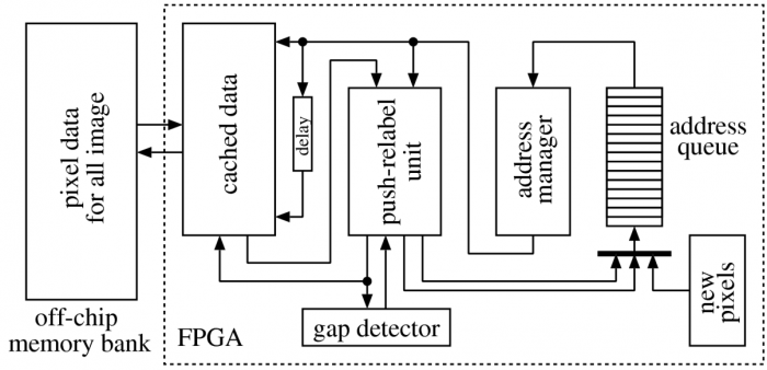
In the Kobori-Maruyama (KM) implementation, they use what is called a "Push-Relabel" GC algorithm. This is a commonly used algorithm because of its speed and its adaptability to highly parallel implementations, such as GPU coding. It's also able to process small chunks of a graph at a time (node by node, only looking at immediate neighbors), so the memory requirements can be kept small. From the presentation and the block diagram, it's apparent that the host system is using the FPGA as an external processor for the image data. The collection of the original data and the use of the results are completely separate from the FPGA.
An example of an FPGA-based implementation for stereo matching GC is a thesis by Havva Ozsarac of the Middle East Technical University in Ankara Turkey.
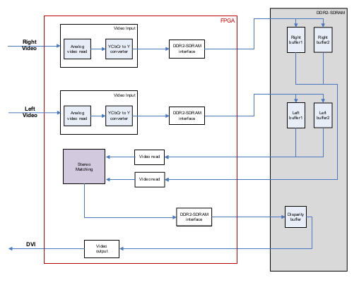
The Ozsarac implementation uses the FPGA to perform simultaneous calculations on pixel groups from two separate video cameras, working through chunks of the image data using a customized GC process to reach real time processing speeds. In effect, the FPGA is processing the stream of video data as it comes into the system, passing straight video to the host computer while also pulling out the information required to perform the GC process. Though there is no Verilog or VHDL code in the paper, the implementations she describes are very detailed at multiple levels.
These two examples showcase the different ways that GC processing can be done. One (KM) is "whole problem" processing, whereby the FPGA is presented with a complete problem to analyze. Conversely, the Ozsarac implementation is stream-based, continuously analyzing the input video frames and presenting an updated output as fast as possible.
Choosing a Design
While both approaches have their merits, as a newcomer to FPGA design, I have decided on an approach that is closer to the KM implementation than the Ozsarac design. Along the way, I hope to gain enough expertise to develop a highly-parallel, stream-based implementation that can handle complex inputs in near real-time. However, what I'll be initially working on is basically a specialized CPU to carry out GC operations. Since "Graph Processing Unit" would just lead to confusion over the acronym (GPU), I'm going to go with a short-hand of "Graph Cut Processing Unit" (GCPU). It seems like a solid approach to begin with.
- Much like a CPU, the implementation will be loaded up with "instructions" (the problem model), and it will carry out a specified series of operations.
- I/O between the host system and the GCPU can be set up like most co-processor implementations.
- Testing and validation should be greatly simplified at each stage.
What the "GCPU" is Supposed to Do
Below is the standard visualization of the GC structure for a 2D image. Planar nodes represent pixels (or positions, in the navigation problem). The two out-of-plane nodes represent the "source" and "sink" of the flow. And the planar links represent edges (connections between nodes), whose capacity values can mean anything from similarity measurements to gallons per minute to amps. In the navigation scenario we're building, the capacities are going to represent collision risk values.
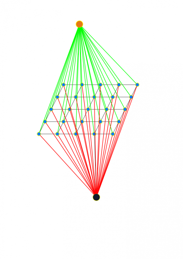
If you spend much time researching GC processes, you'll see this particular representation all over the place. In a way, it has kind of become the obligatory marker for any serious paper in the field. And I don't intend to be dismissive--for anyone working in 2D image processing, it's a good mental model of how you start the problem solving. But the mental model can also be limiting, especially when you're attempting to work specifically outside the realm of 2D image process.
Below is a rearrangement of the standard model. In this layout, an equivalent to a 25 node "image" (square image, 5 nodes per side) is shown. Functionally, the graph structure is precisely the same as the previous model. Each node is connected to the neighboring nodes by edges of various capacity (black lines), and the source and sink nodes are connected by their particular edges (green and red connectors).
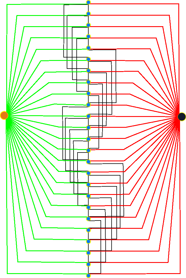
With this particular model, the nodes are listed in increasing order from top to bottom. For each node in the central line, there are 2-4 edges associated with the node. It's a little difficult to see in the image, but every fifth node is missing the direct connection to the next node in the sequence. This is equivalent to the "right" edge not wrapping around to connect to the left edge. The same applies to the top and bottom edges.
For the GC process that I plan on implementing in the GCPU, the solution steps are laid out in the following pseudocode:
declare gc_sum = 0;
declare gc_intermediate = 0;
do {
gc_intermediate = 0;
scan nodes and associate with source or sink;
for each edge that connects node of differing associations:
Find min_flow on path from source to sink;
Apply min_flow to the path;
gc_intermediate += min_flow;
gc_sum += gc_intermediate;
} while (gc_intermediate != 0);
More generically, the internal processes roughly follow this state diagram:
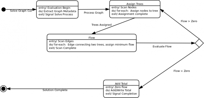
Although there is still plenty of detail to be worked out for the individual steps, the reason for choosing the simpler implementation of a GCPU (rather than a streaming data model) should be apparent. This process is easily shaped into the equivalent of a math processor, such as implementing a Taylor Series to calculate logs or sine/cosine values: Given an input, follow the processing steps until you reach a desired end state, then return the results.
Summary
By looking at other FPGA implementations in the same general problem space, I have decided to take a CPU-like approach to the design. While probably not the most efficient design, the data model and intended algorithm make it easy to break down into components that can be developed and tested individually and together.
Next Steps
At this point, it's still what my old engineering professor would call a "hand waving solution" (lots of words and gestures, few to no real numbers or designs). Not a lot to be excited about, yet, but we're getting there.
Next time, I'll show my (successful?) attempt at implementing the structures necessary to hold the graph model! There will be VHDL, I promise!
- Comments
- Write a Comment Select to add a comment
To post reply to a comment, click on the 'reply' button attached to each comment. To post a new comment (not a reply to a comment) check out the 'Write a Comment' tab at the top of the comments.
Please login (on the right) if you already have an account on this platform.
Otherwise, please use this form to register (free) an join one of the largest online community for Electrical/Embedded/DSP/FPGA/ML engineers:


