


Jumping from MCUs to FPGAs - 5 things you need to know
Are you a microcontroller expert beckoned by the siren song of the FPGA? Not long ago, that was me. FPGA-expert friends of mine regularly extolled the virtues of these mysterious components and I wanted in. When I made the leap, I found a world seemingly very familiar, but in reality, vastly different. My years of C programming and microcontroller use often gave pre preconceived interpretations of FPGA resource material which resulted in eye-roll class mistakes in my code.
If you as of yet, know nothing about FPGAs, you might want to read “How FPGAs work, and why you'll buy one”, by Yossi Krenin and watch “What the FAQ is an FPGA”, by Clive Maxfield first.” Those two articles will give you the basic why’s and what’s of the FPGA. Once you’ve made the choice to go ahead, I have outlined here five of the key things you will need to be aware of when moving from the microcontroller to that of the FPGA.
What’s the same vs. not the same
Many aspects of FPGA development will feel familiar to a microcontroller developer, but some are deceivingly different. You are writing code in a text editor, giving it some processing time and then stuffing it into a chip. The processing and what happens in the chip, however, are vastly different.
Here’s what you will find familiar to your MCU exploits:
- Use an IDE or a command line interface. The basic toolset it very similar. Either you use an IDE that organizes and helps to put together everything necessary, or you use command line instructions to do the same manually
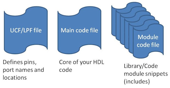
- Multiple files in the development set. As with MCU software, you have a set of different files with different purposes. You have The UCF/LPF (user constraints file/ logical preference file) which is similar to a software header file. There are language code files and finally, modules (AKA includes).
- Multiple language options. As with MCUs, you have multiple language options for FPGAs. There are fewer, but you can choose between a number of options. FPGA languages, such as Verilog, VHDL or MyHDL are called hardware description languages (HDL), not programming languages.
- You code, then implement. As with an MCU, you code and then you implement the code. The implementation is different, but the steps will seem very familiar.
- Often familiar syntax. The syntax in the languages is often very similar. You will find things that look like they come from C, Python and other high level languages. That familiarity, however, can be a trap, which leads me to one of the key differences and the next item in my list.
Item you need to know #1 - You are not writing instructions for a CPU, you are creating hardware.
The FPGA isn’t “running” your compiled or interpreted code. Your code is not a set of instructions for a processing unit. The .bit or .hex file (called the configuration) which is the rough equivalent to object code in the MCU world, is actually describing the physical hardware of an application specific integrated circuit (ASIC). It’s just an ASIC that can change at every power up. That’s why the languages are called hardware description languages (HDL) and not programming languages.
It’s important to note that the fabric inside the ASIC is volatile. FPGA systems have EEPROM or other nonvolatile memory to hold the configuration file while power is off, but in almost all FPGA chips, it must be loaded into the part at power-up. This means you can easily fix problems in the hardware, but it also means that you don’t get an instant on like you do with an MCU. It can take anywhere from a few seconds to a few minutes to get the configuration into the FPGA.
You can implement a CPU in your FPGA fabric and some bigger FPGAs have ARM CPUs built into the package. With either of those scenarios, you will with write code, compile and load it like a conventional CPU/MPU, but that is something separate and different than you FPGA HDL code.
Item #2 - Pin mapping. You define it all.
The I/O pins in a typical FPGA are not connected to anything until you define them. In most microcontrollers, the pins are assigned to peripherals. Many have more than one peripheral and some these days are remapable with a crossbar. In an FPGA, virtually all of the chip pins are that way. Except for power, ground and special function pins, any pin can be mapped to any function. Of course, with an FPGA, you have to create that function in the HDL.
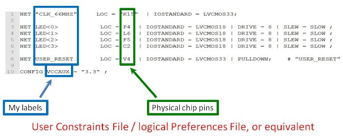
The pin mapping is set up in a special file called a constraints or preferences file. The file is called a UCF, LPF or something similar depending on the chip manufacturer. This file allows you to map a physical chip pin to a label that you specify, and define certain parameters, such as voltage level, input vs output and pull-up/pull-down resisters.
This wondrous feature means that the I/O section of your chip never need end up on the wrong side. If you’ve ever had to route a high speed matched pair of circuit traces from one side of a big chip to the other side where the PCB I/O is, you will appreciate this. You can just map the pins wherever is most convenient.
Item #3 - Clocked circuitry vs. combinatorial logic.
There are two types of logic used inside an FPGA: combnatorial and clocked (also called triggered) logic. This is one of the most important aspects of FPGA development.
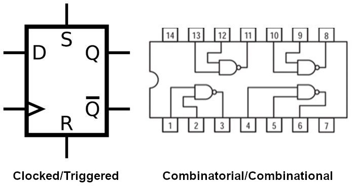
When you wire up digital logic – say a couple of AND gates, NOR gates and such, you are creating what is called combinatorial logic. It is combining the inputs and instantly showing the results of the logic on the output. Instantly minus a tiny amount of propagation delay, that is. In your HDL, you will recognize combinatorial logic by the term “assign.”
assign ExtLEDs[4:0] = freq_div[25:21]; // connects the 4 led outputs to register bits at 25, 24, 23, and 22
Clocked logic is triggered based on a clock pulse (hence the two designations). Nothing happens until a clock pulse hits and whatever processing is inside of that clocked module will always happen, one step with each clock pulse. This is referred to in Verilog as an “always” block. The always block can be triggered on the positive or negative edge of the clock.
always @(posedge clk_in) begin       // Cloked on the rising clock edge
    if(reset)                        // Restart the counter a 0, if the button is pressed
        freq_div <= 0;
    else
        freq_div <= freq_div + 1'd1; // Increment the register by 1
end
Item #4 - Wires and “Registering”.
Blinding flash of the obvious here: Wires just go between two things. Obvious, yes. But it needs to be stated in the “new to FPGA” world. Inside the FPGA, a register is a place to store data or a logic state, A wire connects registers to chip pins or to another register or spot inside of the FPGA.The naming requirements for wires and registers are about the same, so it’s easy for a beginning FPGA user to confuse the two. I once found myself trying to perform a calculation on an input wire. It doesn’t work. Fortunately, the solution is easy and comes in the declaration section of your HDL code.
| 1. Declare your wire | wire LEDout; |
| 2. Declare your register | reg LEDvalue; |
| 3. Assign the wire to the register | assign LEDout = LEDvalue; |
Interestingly, the order of these statements in your HDL code usually doesn’t matter. The synthesizer (which is the software that turns your code into something useable by the FPGA) is creating and placing hardware. Once it’s synthesized, crunched into the bit file and loaded into the FPGA, all of the hardware is in place and ready to go simultaneously. It’s a bit like soldering parts on the a printed circuit board. It doesn’t really matter the order in which you solder them on. They will all be in place when you power the board up.
#5 – Parallel processing.
Again, your FPGA isn’t going through your code line by line. All of the hardware is there and ready to go. Any combinatorial logic, identified by the “assign” statement, is operates in real time. Whenever a value is on the input, the output immediately (plus any propagation delay) reflects the results of the logic circuitry.
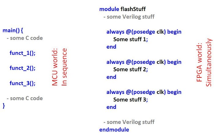
Anything that is clocked circuits, identified by being within an “always” block will operate at the same time as anything else that shares the same clock.
What next?
There is so much more to an FPGA than what I have covered. In fact, if you check back, I’ll have a second installment of this article covering a few more of the issues that tripped me up due to my microcontroller mindset. In the meantime, there is a wealth of information on embeddedrelated.com on the subject. I recommend that you find yourself an inexpensive FPGA development board and take the plunge.
Duane Benson
- Comments
- Write a Comment Select to add a comment
To post reply to a comment, click on the 'reply' button attached to each comment. To post a new comment (not a reply to a comment) check out the 'Write a Comment' tab at the top of the comments.
Please login (on the right) if you already have an account on this platform.
Otherwise, please use this form to register (free) an join one of the largest online community for Electrical/Embedded/DSP/FPGA/ML engineers:


