VHDL tutorial - part 2 - Testbench
Quick Links
- Part 1: VHDL tutorial
- Part 2: part 2 - Testbench
- Part 3: combining clocked and sequential logic
- Part 4: Creating a hierarchical design
- Part 5: A practical example - part 1 - Hardware
- Part 6: A practical example - part 2 - VHDL coding
- Part 7: A practical example - part 3 - VHDL testbench
In an earlier article I walked through the VHDL coding of a simple design. In this article I will continue the process and create a test bench module to test the earlier design. The Xilinx ISE environment makes it pretty easy to start the testing process. To start the process, select "New Source" from the menu items under "Project". This launches the "New Source Wizard". From within the Wizard select "VHDL Test Bench" and enter the name of the new module (click 'Next' to continue). The "New Source Wizard" then allows you to select a source to associate to the new source (in this case ClkDiv from the prior article), then click on 'Next'. The Wizard then creates the necessary boilerplate for a test bench module (see below).
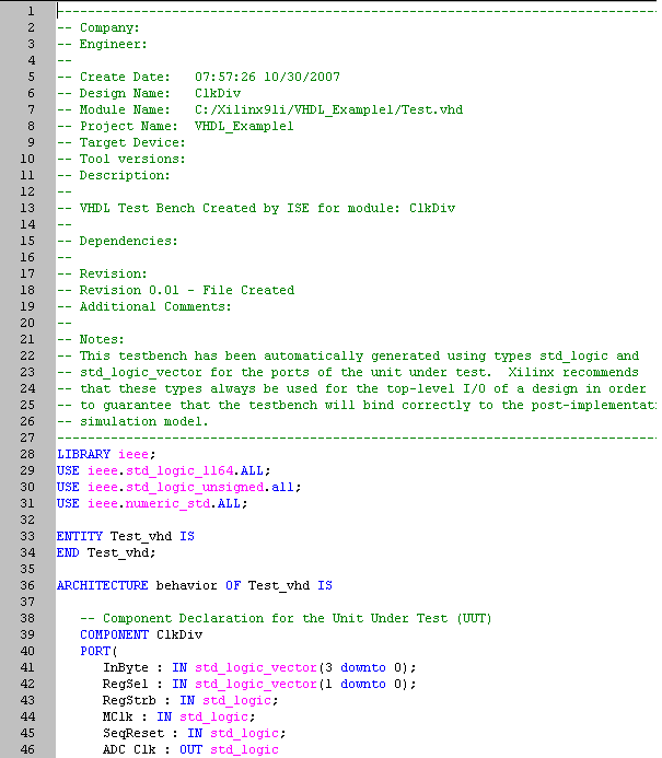
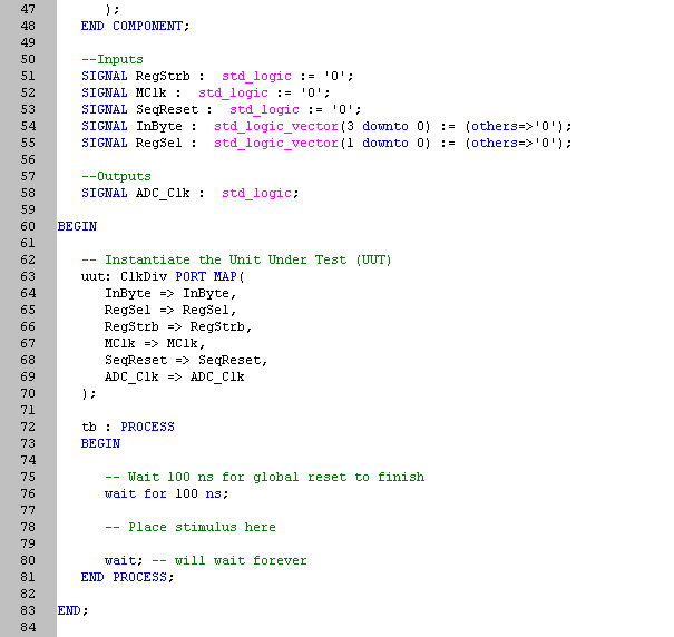
The boilerplate includes the component declaration section (lines 38-58) and the instantiation of the test (lines 62-70). The boilerplate also includes a stub for the main test process (tb:PROCESS, lines 72-81). It is our job to turn this simple stub into an actual test sequence that will exercise our design.
The first step in the design of the test bench is to create a continuous clocking signal for the master clock (MCLK). VHDL provides a simple way to create repetitive signal. This is done in the following code fragments.
![]()

The first statement (line 60) defines a constant that is equal to half the period of the master clock. The remaining lines (74-48) create a process that toggles the master clock (MCLK). MCLK is driven low after the first 12.5ns and driven high after the next 12.5ns. This process waits a total of 25ns and then repeats. This sequence of steps creates a master clock signal of 40MHz.
The next step is to establish the initial conditions for the device and to generate a reset pulse. The following statements show this sequence.

In the above figure, Lines 80-81 open the testbench process (tb). The first delay (line 84, wait for 100 ns) allows for the power on reset action within the CPLD to complete. Following that statement, we establish the initial conditions for the device (line 86, note: SeqReset is drive low). After 100ns (line 87), the device is removed from reset (line 89) and allowed to run. The default clock rate is in effect and can be observed by pausing the testbench process and allowing the device to run (line 90, wait for 1 μs).
Now might be a good time to look at some data. Simulating the above statements, we can check to see if the data is beginning to look as we expect it.

Looking at the data, starting at time zero, we can see the MCLK toggling with SeqReset held low. At the first major timing mark (200ns) we can see SeqReset being driven high and the adc_clk soon starting to toggle (half period of 500ns, or the expected 1MHz rate). So far, so good.
The next step in the process is to write to the clock divisor (RegSel = '01', InByte = rate selection, RegStrb = '0' then RegStrb = '1'). After the necessary delays (for RegStrb and allowing the clock divisor to run), we can repeat the sequence for each of the clock rates. The following code fragment shows these sequences.
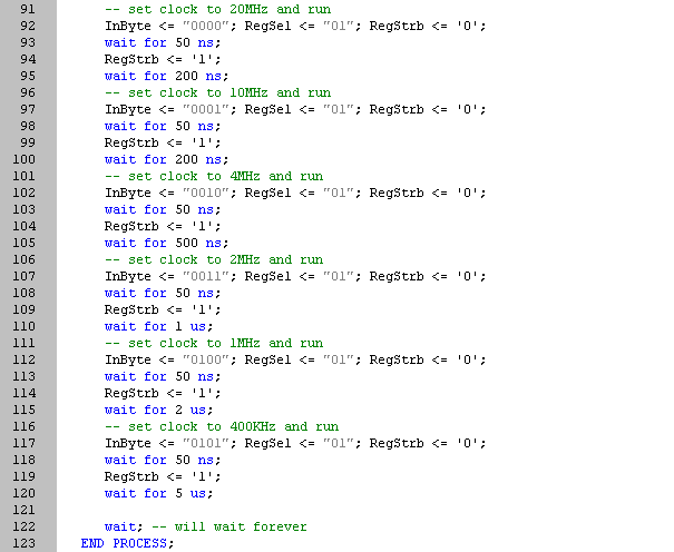
For each of the target clock rates we need to repeat the basic sequence of setting up the clock select register (Inbyte) and register select (RegSel) values and the toggling the RegStrb line (i.e. lines 92-94). We also need to allow time for the selected clock rate to be observed (i.e. line 95). These statements are then repeated for each clock rate (remembering to increase the 'observation' wait time for each new clock rate)
Now we can look at the completed results.

At each clock selection point (toggling of RegStrb) we see a change in the outpur clock rate (Adc_Clk). It was a good thing that I tested this code. During the generation of this test bench, I found that I had made a mistake in my earlier VHDL code (cut and paste, but no change in the data on line 48 and 50). In the previous article the ClkDiv process was written as:
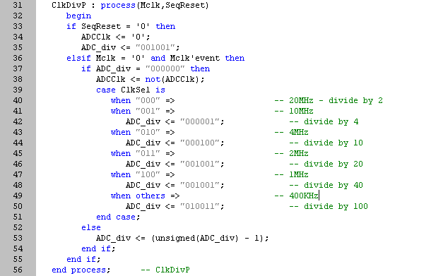
In testing, I found that I needed to correct the ClkDiv process to:
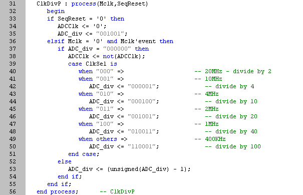
It only goes to show, that if you haven't tested it, it probably doesn't work.
In a future article, I will show some of the more advanced programming techniques of VHDL.
Again, Happy designing!
Gene
- Comments
- Write a Comment Select to add a comment
To post reply to a comment, click on the 'reply' button attached to each comment. To post a new comment (not a reply to a comment) check out the 'Write a Comment' tab at the top of the comments.
Please login (on the right) if you already have an account on this platform.
Otherwise, please use this form to register (free) an join one of the largest online community for Electrical/Embedded/DSP/FPGA/ML engineers:


