


How to Read a Power MOSFET Datasheet
One of my pet peeves is when my fellow engineers misinterpret component datasheets. This happened a few times recently in separate instances, all involving power MOSFETs. So it’s time for me to get on my soapbox. Listen up!
I was going to post an article on how to read component datasheets in general. But MOSFETs are a good place to start, and are a little more specific. I’m not the first person to write something about how to read datasheets; here are some other good articles:
- How to Read a Datasheet, Michigan State University ECE480
- How to Read a FET Datasheet, University of Nevada Las Vegas PHYS483
- A Complete Guide to Data Sheets, F. Raymond Dewey, Allegro Microsystems
- How to Read a Datasheet, David Kress, Analog Devices
- AN11158: Understanding power MOSFET data sheet parameters, NXP
- Infineon OptiMOS Power MOSFET Datasheet Explanation, Alan Huang, Infineon Technologies
What Is a Datasheet?
This may be a dumb-sounding question, but what is a datasheet, exactly? It’s a document that describes the behavior, appearance, performance, and limitations of a component, as asserted by the manufacturer.
Okay, so what does that mean?
Well, you really have to read the fine print. The information in a datasheet — for example, that the IRFP260N’s RDS(on) has a maximum of 0.04 Ω at VGS = 10V, ID = 28A at a junction temperature of 25°C, — is an assertion, a claim. It is not a warranty or guarantee unless the manufacturer says so, and for that kind of a thing, (a) you have to read the fine print, and (b) I am not a lawyer, so don’t take my advice as gospel, seek your own legal counsel. Each of the semiconductor manufacturers has their own fine print, for example here are excerpts from some of them:
Fairchild:
FAIRCHILD SEMICONDUCTOR RESERVES THE RIGHT TO MAKE CHANGES WITHOUT FURTHER NOTICE TO ANY PRODUCTS HEREIN TO IMPROVE RELIABILITY, FUNCTION, OR DESIGN. FAIRCHILD DOES NOT ASSUME ANY LIABILITY ARISING OUT OF THE APPLICATION OR USE OF ANY PRODUCT OR CIRCUIT DESCRIBED HEREIN; NEITHER DOES IT CONVEY ANY LICENSE UNDER ITS PATENT RIGHTS, NOR THE RIGHTS OF OTHERS. THESE SPECIFICATIONS DO NOT EXPAND THE TERMS OF FAIRCHILD’S WORLDWIDE TERMS AND CONDITIONS, SPECIFICALLY THE WARRANTY THEREIN, WHICH COVERS THESE PRODUCTS.
NXP:
General — Information in this document is believed to be accurate and reliable. However, NXP Semiconductors does not give any representations or warranties, expressed or implied, as to the accuracy or completeness of such information and shall have no liability for the consequences of use of such information.
Vishay:
Vishay disclaims any and all liability arising out of the use or application of any product described herein or of any information provided herein to the maximum extent permitted by law. The product specifications do not expand or otherwise modify Vishay’s terms and conditions of purchase, including but not limited to the warranty expressed therein, which apply to these products.
TI:
TI warrants performance of its components to the specifications applicable at the time of sale, in accordance with the warranty in TI’s terms and conditions of sale of semiconductor products. Testing and other quality control techniques are used to the extent TI deems necessary to support this warranty. Except where mandated by applicable law, testing of all parameters of each component is not necessarily performed
Microchip:
Information contained in this publication regarding device applications and the like is provided only for your convenience and may be superseded by updates. It is your responsibility to ensure that your application meets with your specifications. MICROCHIP MAKES NO REPRESENTATIONS OR WARRANTIES OF ANY KIND WHETHER EXPRESS OR IMPLIED, WRITTEN OR ORAL, STATUTORY OR OTHERWISE, RELATED TO THE INFORMATION, INCLUDING BUT NOT LIMITED TO ITS CONDITION, QUALITY, PERFORMANCE, MERCHANTABILITY OR FITNESS FOR PURPOSE.
And IR’s datasheets don’t really say anything other than “Data and specifications subject to change without notice.”
So what’s an engineer to do? The best I can make sense of this — and again, I am not a lawyer — is that a datasheet is essentially a confident assertion of information about a device, but with no legal guarantee backing it up, at least not from the datasheet.
For example, IR is confident that if you raise the gate voltage 10V above the source voltage of the IRFP260N, and you let 28A flow from drain to source at a 25°C junction temperature, then the on-resistance will be no more than 0.04 Ω. In practice, what this means is that the manufacturer performs characterizations and tests, sometimes on each and every component it manufacturers, sometimes not. This gives them histograms of the performance characteristics of the devices they manufacture. If they test each device and they find one that exceeds the limits, it gets discarded. The manufacturer has enough information so that, in a statistical sense, the probability is very small that a device will have any characteristics that exceed the datasheet specifications. They won’t tell you that probability. But it’s small; maybe 1 out of a billion devices might exceed the specifications.
If you do want a legal guarantee, then it has to be part of the terms and conditions of sale, when you buy the parts from the manufacturer. If you’re a large company and you buy millions of dollars worth of parts from a semiconductor manufacturer, maybe you can negotiate a warranty. The rest of us (and more often than not, we don’t even buy directly from the manufacturer; we buy from distributors) just have to trust the manufacturers. Phooey.
On the flip side, semiconductor manufacturers do want to stand behind their brand identity, so if you find a part that doesn’t meet its specifications, they’ll want to know so they can figure out why, and make sure it doesn’t happen again. But chances are you haven’t followed all the rules in the datasheet; maybe you’ve overheated the device, or zapped it with an electrostatic discharge. And in that case all bets are off — once you’ve exceeded the ratings, there’s no guarantee that the device will work. I’d be willing to bet you lunch any day of the week that the part meets the specs in the datasheet.
All right, enough of the legal crap. Remember, I am not a lawyer.
A few examples
Just for something more tangible, let’s look at a few MOSFET datasheets. All of these are N-channel devices:
- IRFP260N (200V 40mΩ TO-247AC), International Rectifier (now part of Infineon)
- FQA70N15 (150V 28mΩ TO-3PN), Fairchild Semiconductor
- SUP85N15 (150V 21mΩ TO-220AB), Vishay Siliconix
- PSMN035-150P (150V 35mΩ TO-220AB), NXP
- MCP87130 (25V 13.5mΩ 5x6-PDFN), Microchip Technology
- CSD18542KCS (60V 3.3mΩ TO-220), Texas Instruments
The first three of these documents follow the “classic” MOSFET datasheet format that International Rectifier introduced in the 1980s with its HEXFET line of devices. The IR MOSFET datasheet is an 8-page document that describes, in almost liturgical regularity, all the information the manufacturer wants you to know about a particular device.
Pie Jesu Domine
Rdson is seven ohms....
A MOSFET datasheet from IR contains these sections, in this order:
- A general description including voltage, on-resistance, current ratings and package information
- A table of absolute maximum ratings
- A table of thermal resistance parameters
- A table of electrical characteristics
- Figures, including
- Graphs of typical characteristics
- Diagrams of test circuits
- Package information
Most MOSFET manufacturers used to follow this organization. An 8-page datasheet is kind of nice, because if you have favorite components, you can print them out as 2-up double-sided documents on two pages of paper, and put them in a three-ring binder. Call me old-school, but I can read a datasheet more easily on paper than on a computer screen.
Then Philips Semiconductor (now NXP) broke the convention and did their own thing. The same kind of stuff is in NXP’s datasheets, but it’s in a different order and therefore not as easy to compare side-by-side if you are trying to select a MOSFET. Phooey on them.
The Specification Game
Okay, now it’s time to play the Specification Game.
There are several types of information in a datasheet. Some of these don’t involve performance specifications, so we’re not going to talk about them here:
- part numbering information: for example, part number suffix TR might indicate tape-and-reel, or suffix Q might mean automotive qualified.
- package information: for instance, the package is a TO-247AC, marked in a certain way.
- behavioral specifications: Microcontrollers are full of these; for example, addresses 0x4000 and 0x4002 contain the 16-bit registers
TMRFOOandTMRBAZwhich dictate the timer periods of the FOO and BAZ timers. MOSFET datasheets don’t contain these types of specs; instead, a MOSFET is an abstract concept that has certain general behaviors. Manufacturers endeavor to maintain these behaviors, and often publish separate application notes about them. For example:- IR AN1084 Power MOSFET Basics
- IR AN936 The Do’s and Don’ts of Using MOS-Gated Transistors
- IR AN937 Gate Drive Characteristics and Requirements for HEXFET® Power MOSFETs
- IR AN941 Paralleling Power MOSFETs
- IR AN944 Use Gate Charge to Design the Gate Drive Circuit for Power MOSFETs and IGBTs
- IR AN947 Understanding HEXFET® Switching Performance
- IR AN949 Current Ratings of Power Semiconductors and Thermal Design
- IR AN957 Measuring HEXFET® MOSFET Characteristics
- IR AN976 Understanding and Using Power MOSFET Reliability Data
- IR AN1005 Power MOSFET Avalanche Design Guidelines
- IR AN1012 Mounting Considerations for International Rectifier’s Power Semiconductor Packages
- IR AN1040 System Simulation Using Power MOSFET Quasi-Dynamic Model
- Fairchild AN558 Introduction to Power MOSFETs and their Applications
- application information: National Semiconductor datasheets contain probably the best examples of application information — little snippets of sample circuits for op-amps and voltage regulators. Look at p. 15-23 of the LM358 datasheet, for example. MOSFET datasheets don’t have these.
- legal information
- contact information (manufacturer’s address/phone number/website)
- noncommittal marketing fluff (”Fifth Generation HEXFETs from International Rectifier utilize advanced processing techniques to achieve extremely low on-resistance per silicon area. This benefit, combined with the fast switching speed and ruggedized device design that HEXFET Power MOSFETs are well known for, provides the designer with an extremely efficient and reliable device for use in a wide variety of applications.”)
The remaining bits of information fall into one of four categories. I’ll show an example of each of these from the IRFP260N datasheet:
- marketing summary
- absolute maximum ratings
- specifications
- characterization graphs
Welcome to the Specification Game! First you’ll see the marketing summary. The marketing summary is what shows up at the top of the datasheet. It’s there to contain a few key excerpts from the detailed specifications mentioned later. Do not trust anything listed here unless you can verify it in later specifications.
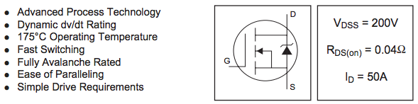
These are informal statements. They are not specifications, because there isn’t enough information here to tell what they’re saying. For instance, the “VDSS = 200V” means that the drain-to-source breakdown voltage is a minimum of 200V at a given current and temperature, but you’re not going to find those details unless you look in the specifications. Some manufacturers show typical values, some show minimum or maximum.
The next section covers the absolute maximum ratings of the device.
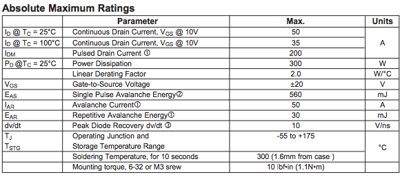
This is a table telling you a bunch of things you can’t do, if you expect the device to work. If you exceed any of these at any time, Game Over. In that case, the manufacturer will not make any guarantees for device behavior at any time after the absolute maximum ratings have been exceeded. The MOSFET could be damaged. It might work fine. It might work with reduced performance. It might turn green, or start dancing around, whispering “Rosebud!”, although this is rather unlikely. You just don’t know. In the case of the IRFP260N, there are 13 line items. I’ll go over these in more detail later in this article.
So to play the Specification Game, you have to be willing to make sure that the maximum ratings are never exceeded. NEVER.
And even then, there might be circumstances in which the device won’t meet its remaining specifications: for example, exposure to radiation, or chemicals, or electrostatic discharge, or excess humidity.
The next section is the most important one, the table or tables of specifications.
Specification tables have three important pieces of information:
- a description (symbol and name) of a parameter
- a numerical specification, including units
- the conditions under which the specification is valid.
The description tells you what the parameter is, and as long as you know something about MOSFETs, then these have more-or-less standard meanings.
The numerical specification tells you one of three things. If it’s a minimum or maximum, it’s an asserted limit, and if you trust the manufacturer (you should in most cases) and you’ve stayed within all the absolute maximum ratings, then you can expect that your device behavior will be above or below the specified limit. Great!
If the numerical specification is a typical value, this doesn’t really tell you much, just a warm-and-fuzzy number that the manufacturer suggests using in some cases, because you’re not going to get anything better. (Sorry.) In some cases, it is a mean value from characterization data, but manufacturers will rarely state that. Values marked “typical” do not represent limits, and any particular device may differ from the typical values. For example, look at the drain and source inductance values, listed as 5.0nH and 13nH typical. If you want to make some rough estimations of device behavior, sure, go ahead and use these values. If you have to depend on drain and source inductance, tough luck — you’ll have to measure these values on your own somehow; one device might have 2nH drain inductance and another might have 11nH drain inductance. We just don’t know. If you have a good relationship with the manufacturer (meaning you buy or plan to buy lots of their products) then perhaps you can persuade them to give you a copy of some of the characterization data they have… perhaps they tested 50 devices and the mean value of drain inductance was 5.0nH, and all devices were between 4.5 and 5.5nH. We don’t know, and the manufacturer has decided not to make any claim on minimum or maximum inductance. Most likely it’s just because it’s too expensive to test on every device.
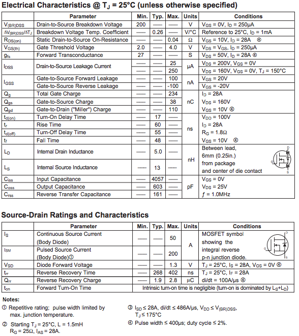
The last important thing about a specification is the set of conditions under which that specification is valid. These are the qualifications for the numerical spec. For example, the RDS(on) limit of 0.04 Ω is not guaranteed unless you comply with the conditions of the spec: The junction temperature TJ must be 25°C (this is typical for most specs), the gate-to-source voltage must be 10V, and the drain current must be 28A. If you conduct 29A into the device, all bets are off; same if the junction temperature is 30°C, or if the gate-to-source voltage is 9.5V. In all three of these cases, on-resistance will be higher.
Finally, the datasheet includes a section full of pretty characterization graphs:
These show all sorts of useful information, but what you need to remember is that unless otherwise stated, these are always TYPICAL. They do not represent any kind of a specification. You can only use them for learning about general qualitative behavior. If you need anything definitive, you cannot rely on them. They may represent the mean value of a large number of sample devices. They may represent the measurement of only one particular sample, the one that Test Engineer Bob happened to have on his desk the day his boss said they needed characterization data for the datasheet.
Thank you for playing the Specification Game! Remember that marketing summaries don’t matter, typical specifications don’t matter, characterization graphs don’t matter… only the minimum and maximum specifications matter, as long as you meet all the conditions and don’t exceed the Absolute Maximum Ratings.
Practicalities of Datasheets
Whoa. This sounds kind of cynical. I can’t trust half of what’s in the datasheet? Really?!
The trick is to learn when to rely on information in the datasheet, and how to use it for what purposes. Essentially, unless a number is part of a minimum or maximum specification, you cannot use it without doing your own independent validation.
For example, take the normalized on-resistance vs. temperature graph.
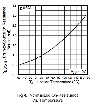
Here’s the weird thing. You know that RDS(on) number, 0.04 Ω, we’ve been carrying around? It is a maximum specification in the datasheet. But it’s got a condition of 25°C junction temperature. And almost nobody operates a MOSFET with the junction at 25°C. You might be using it at room temperature ambient, but the device will heat up, and usually the junction temperature is above 25°C. Let’s say I know it’s at 100°C junction temperature. I use figure 4 to decide that at 100°C the on-resistance will be a factor of 1.8× higher, or 0.072 Ω. That’s probably accurate… but if I need to rely on it, I need to make my own measurements to confirm it.
Sometimes you learn with experience which device parameters have a lot of part-to-part variation, and which ones will tend to tightly cluster around the mean. It’s not something that will be stated in the datasheet; you’ll have to read the manufacturer’s appnotes, contact their applications department, or do your own tests to make those kind of conclusions.
The Important Stuff: MOSFET Specs You Need to Know
There are a lot of numbers in the absolute maximum and specification tables. Here are the ones you really have to know first and foremost.
- Operating Junction and Storage Temperature Range. This is the most important item in the absolute maximum ratings list. Most of the other items you will never run into. For the IRFP260N it’s -55 to +175 °C. Unless you’re working with aerospace issues, you probably won’t have to worry about the -55°C limit. That leaves +175 °C. Most MOSFETs are rated either at a maximum +150°C or +175°C junction temperature. Do your thermal design properly, and leave some margin, and you can make sure you meet this requirement.
- Junction-to-Case thermal resistance RθJC. A thermal resistance of 0.50 °C/W means that for each watt of power dissipated in the junction, the junction temperature will rise 0.5 °C above the case temperature. In other words, \( T_J = T_C + R_{\theta JC}P_J \) where \( P_J \) is the power dissipated in the junction.
- Drain-to-Source Breakdown Voltage. A MOSFET can be used in a controlled fashion below the breakdown voltage. This spec says as long as I keep the voltage across drain-to-source below 200V, the drain current will not exceed 250μA. As soon as I go above 200V, all bets are off. In practice, because MOSFETs are used as dynamic switches, we don’t usually use a 200V MOSFET up to its full rated voltage; instead, we use some kind of derating to make sure that the inductive spikes during switching transients don’t exceed the breakdown voltage. Derating in the 60-70% range seems to be the norm; if I wanted to use a system with DC voltage up to 48V, I would use MOSFETs with a breakdown voltage rating of at least 75V. A 60V MOSFET doesn’t have enough design margin to handle inductive spikes from a 48V source.
- Static Drain-to-Source On-Resistance RDS(on). This is generally the most important performance characteristic. After all, you’re using the device as a switch, and you want to make sure that the voltage drop across the switch is acceptable given a specific current level. Remember that the gate-to-source voltage VGS and drain current are conditions of the spec. Most “regular” power MOSFETs are specified at 10V VGS; some logic-level MOSFETs are specified at 4.5V or 5V VGS; occasionally you’ll find low-voltage MOSFETs specified at somewhere in the 1.8 - 3.3V VGS range. If you are using a MOSFET as a switch and cannot meet the on-resistance spec, don’t use it!!! This means that if you have a logic level output from a 3.3V system, you should NOT be using MOSFETs spec’d at 4.5V. There’s not enough voltage to guarantee a full turn-on. Don’t forget that just because you use “5V” logic, it doesn’t mean your output high voltage will be 5V. That’s why logic-level MOSFETs are generally specified at 4.5V Vgs, so that you can make sure your output high level is above this threshold. I have seen this mistake over and over and over. If you can’t meet the Vgs spec, the drain-to-source resistance generally will be higher than the RDS(on) spec. It may not behave in a resistive manner at all; at lower Vgs levels, the MOSFET behaves like a constant-current sink, with the exact amount of current highly dependent on part-to-part variation and junction temperature.
- Gate Threshold Voltage VGS(th). This is important only because you should know what it does mean and what it doesn’t mean. The gate threshold voltage is not some magic voltage above which the MOSFET is considered “on”. It is a voltage at which the MOSFET just barely starts to conduct. The IRFP260N lists 2.0-4.0V for a drain current of 250uA. If you look at this spec and conclude that a VGS of 4.5V is sufficient to turn the device on, you are WRONG. You need the full 10V. What the gate threshold voltage is useful for, however, is making sure the device is off. Ideally you want zero voltage between gate and source to hold the MOSFET off. But no gate driver is perfect in that regard. It has static and dynamic characteristics that will have some small nonzero voltage drop above its return supply rail. So if I’m using a logic chip that can sink to 0.5V or even 1.5V, that might be acceptable to turn a MOSFET off, because it’s below the minimum gate threshold of 2.0V, and therefore less than 250uA of current will flow. Note that for power applications, this may be fine, but for signal applications, 250uA is a large number, and most MOSFETs don’t do a good job staying completely “off”.
- Gate Charge. These specifications are really important numbers. MOSFET gates are capacitive, and its characteristic capacitances are very nonlinear with voltage, but you can use the charge to calculate worst-case switching times. Gate charge determines how fast the MOSFET will switch from ON to OFF and back. If you know the gate driver current, just divide total gate charge by the current. If I have a 1A gate driver, 234nC will take up to 234ns to turn completely on or off. The gate-to-drain (“Miller”) charge tells me roughly how fast the MOSFET will go through its linear region and its drain voltage will rise or fall. That 1A gate driver will take up to 110ns to charge or discharge the gate-to-drain capacitance with its 110nC maximum specification. The gate charge specifications are generally much more useful than the capacitance specs (input/output/reverse transfer), since the latter are usually typical and usually measured only at zero gate-source voltage, and these are very nonlinear capacitances.
- Turn-on, Rise, Turn-off, and Fall times. These are useful only for understanding the minimum switching times. Usually your gate drive circuit won’t switch as fast as these numbers anyway, so they’re helpful but only as a rough frame of reference.
That’s really it! The rest of the specs are for more advanced calculations and you probably won’t use them.
For example, the “Forward Transconductance” rating gfs is something I’ve never used in 20 years of experience dealing with MOSFETs. Forward transconductance is the linear relationship of drain current to gate voltage; a minimum of 27S = 27A/V at ID = 28A and VDS = 50V means that when the gate-to-source voltage is just barely enough to support 28A drain voltage, then if you increase the gate voltage by an additional 1mV, the drain current increases by at least 27mA. Okay. Sure. Whatever. It’s just that this spec takes place in the linear region, with 1400W being dissipated in the device. So it will tell you something about how the drain current changes during switching, when the gate voltage is increasing above the threshold voltage, but the spec is only at one particular operating point, so it’s really not useful in practice.
If there’s a spec in the datasheet you’re interested in, or find useful, that I haven’t covered, I’d love to hear about it!
Important Characterization Graphs
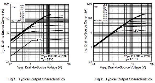
We’ve already seen Figures 1 and 2:
They represent typical device behavior at 25°C and 175°C. For a given gate-to-source voltage, MOSFETs have four important regions of operation, two of which are not shown here.
- If drain-to-source voltage is negative, the body diode conducts.
- If drain-to-source voltage is positive but sufficiently low, the MOSFET acts like a resistor. In a log-log graph, this shows up as lines where the slope is 1. (in Fig. 1, this is shown for VGS = 4.5V up to about 1.1V VDS; for VGS ≥ 8.0V it’s true up to about 10V VDS)
- If drain-to-source voltage is high but below the breakdown voltage, the MOSFET acts like a constant current sink. This shows up in the graphs as horizontal lines.
- If drain-to-source voltage is above the breakdown voltage, anything can happen; the MOSFET is likely to conduct.
Figure 2 is just telling you how things can change at elevated temperatures. Don’t forget: These are typical graphs and you cannot rely on them to decide “Oh, well, I have a gate driver that can only put out 8V, that’s good enough.” Make sure you meet the RDS(on) specification by ensuring you have sufficient voltage!!! If the spec says you need 10V, you need 10V.
I’ve already mentioned Figure 4, which gives normalized on-resistance vs. temperature. Multiply this factor times the RDS(on) value at 25°C and you can figure out the approximate on-resistance at elevated temperatures. The upward concavity of the graph means that in some cases MOSFETs that see constant current loads (or are used to regulate constant current) can see thermal runaway: increased junction temperature causes increased on-resistance, which increases the power dissipation, which increases the junction temperature further. Yikes. Be careful.
Figures 5 and 6 have to do with the gate capacitance:
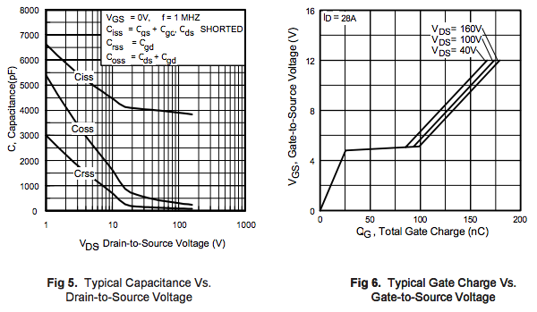
Figure 5 shows the nonlinear decrease of capacitances with increasing drain-to-source voltage.
Figure 6 shows the typical gate charge vs. gate-to-source voltage graph. The left slope of the graph represents the initial turnon before the gate threshold is reached. The plateau in the graph represents when drain current is enough to start pulling the drain terminal down in voltage. This is a plateau because it stays roughly at constant drain current (= constant gate-to-source voltage) while the drain terminal voltage is decreasing. Then, once the drain voltage has dropped to a minimum and the MOSFET has been turned fully on, further increases in gate charge correspond to increases in gate-to-source voltage. Again, do not rely on this graph to determine whether gate-to-source voltages are sufficient. If I did that, I would conclude that 5V is enough. That may be true for one particular sample, but it won’t be true for all devices. Use the RDS(on) spec to ensure your gate-to-source voltage is sufficient.
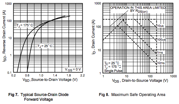
Figure 7 just shows the typical diode characteristic for reverse drain currents.
Figure 8 is very important for looking at fault conditions. Unlike the other graphs, it is not a typical characterization graph. This graph represents the maximum safe operating area (SOA) of a single pulse. At any given instant, the MOSFET should stay within the region marked by the dotted lines. If I have a 10A pulse of current conducting for 10ms with 10V across drain-to-source, that’s within the SOA. If I had 100A for 10ms with 10V across drain-to-source, that’s too high. During static conduction, you won’t see these types of conditions; the upward-sloping line on the left represents the resistive characteristics of when the MOSFET is fully turned on. Operation to the right of this line means the MOSFET is switching on or off, or is not sufficiently turned on. The graph means that the MOSFET can handle a fault condition of 100A and 200V drain-to-source for up to 10μs. If you turn on a MOSFET across a 200V capacitor and 100A flows, then it can withstand the fault condition as long as you can turn it off within 10μs. This can happen in a half-bridge if one of the transistors is shorted.
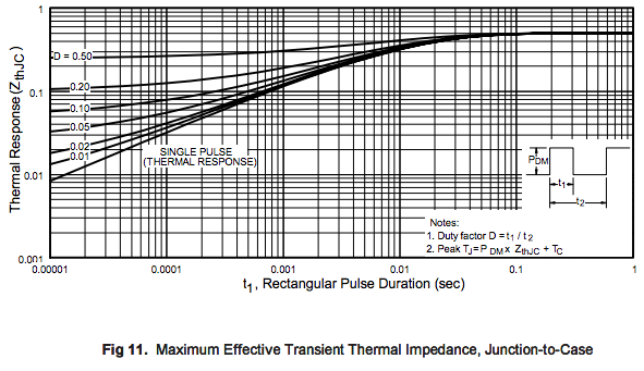
Finally, figure 11 shows the maximum effective thermal impedance. This is what you can use to calculate junction-to-case thermal rise in dynamic conditions, when the MOSFET is turning on or off. For instance, suppose the MOSFET is repetitively conducting 10A during a 20% duty cycle switching waveform at 100μs switching period. That’s an on-time of 20μs and an off-time of 80μs. If I find the D=0.20 curve at 20μs, I see a thermal response ZthJC of about 0.11°C/W instead of the continuously-on value of RθJC of 0.5°C/W mentioned in the thermal resistance part of the specifiction. Makes sense: at high switching frequencies, the MOSFET sees only the average conduction power, because the thermal characteristics of the device act like a low-pass filter. At low switching frequencies (here the breakpoint is about 10 milliseconds on-time) instead of a low-pass filter, the junction heats up when the MOSFET turns on, and the junction cools off when the MOSFET turns off.
That’s about all I have to say about thermal characteristics of MOSFETs, which I’ve covered in another article.
Wrapup
We’ve covered the bulk of the content of the classic power MOSFET datasheet. Here’s what it boils down to:
- Datasheets contain lots of useful advisory information, but they are not a legal guarantee.
- Absolute maximum specifications are what you must meet if you are using a particular component; the remaining specifications are not valid at any time after you have violated the absolute maximum specifications, even if it’s only for an instant.
- Minimum and maximum specifications are the only other part of a datasheet that you can rely on. (They’re practical guarantees even if they’re not legal guarantees.)
- Unless otherwise specified, characterization graphs show typical values — you might learn qualitative behavior from them, but you can’t rely on them in a quantitative sense.
- When using a power MOSFET as a switch, do not rely on its behavior unless you provide a gate-to-source voltage Vgs that is at least one of the values mentioned in the Rds(on) specification. Gate-to-source voltages below these values are not enough to ensure the device works properly as a switch.
- For further information about power MOSFETs, see the application notes published by the manufacturer.
I’ve also covered power MOSFETs in a number of other articles:
- Byte and Switch (Part 1)
- Byte and Switch (Part 2)
- Which MOSFET Topology?
- Hot Fun in the Silicon: Thermal Testing with Power Semiconductors
Happy switching!
© 2015 Jason M. Sachs, all rights reserved.
- Comments
- Write a Comment Select to add a comment
where can i find the Vgs that open the transistor completely (as short circuit)?, you said that the Vgs in the maximum table shouldn't be used
Btw. Jason, id like to ask when the part III of velocity estimation article series finally comes out.
Thanks in advance :)

Thank you for useful article. Can you please reply what will happen when I apply voltige much above of threshhold but smaller of source-drain voltage to the gate of a mosfet and bipolar transistor? In first case I assume it break isolation of a mosfet. Bipolar transistor have insted of it pn-junction. How much voltage can I apply without risk of breaking it to this transistors? Can you say? Thanks in advance.
I'm not sure exactly what your question is... the datasheet will tell you, in the Absolute Maximum section, the allowable gate-to-source voltage range.
For the IRPF260N, for example, Vgs (Gate-to-Source Voltage) has a maximum range of ± 20V. This is pretty typical for most MOSFETs, however it can vary from part to part. (I had to search hard to find one that wasn't ±20V max; the Rohm RE1C002UN is an example rated for 8V.)
As long as you stay within that range you are fine; if you exceed those ratings for even a microsecond then the part may undergo permanent damage.
Thanks again. I'll look datasheet of a bipolar to be sure. About mosfets I was certain, because they have very thin oxide isolation.
I know this may sound dumb,..here i got an Mosfet IRFZ44N X912D B9P0..I want to know what's this numbers stands for..and how do I find an mosfet whether its logical or power mosfet with these numbers..?
To post reply to a comment, click on the 'reply' button attached to each comment. To post a new comment (not a reply to a comment) check out the 'Write a Comment' tab at the top of the comments.
Please login (on the right) if you already have an account on this platform.
Otherwise, please use this form to register (free) an join one of the largest online community for Electrical/Embedded/DSP/FPGA/ML engineers:


