


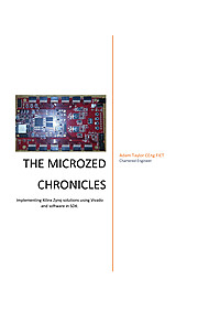
Adam Taylor's MicroZed Chronicles
This is a collection of a number of blogs I have written for the Xilinx Xcell Daily blog on how to use the Xilinx Zynq based around the MicroZed.
The Shock and Awe VHDL Tutorial
The purpose of this tutorial is to provide students with a guide to help develop the skills necessary to be able to use VHDL in the context of introductory and intermediate level digital design courses. These skills will allow students to not only navigate early courses, but also give them the skills and confidence to continue on with VHDL-based digital design and the development of skills required to solve more advanced digital design problems.
VHDL Tutorial
The purpose of this tutorial is to describe the modeling language VHDL. VHDL includes facilities for describing logical structure and function of digital systems at a number of levels of abstraction, from system level down to the gate level. It is intended, among other things, as a modeling language for specification and simulation. We can also use it for hardware synthesis if we restrict ourselves to a subset that can be automatically translated into hardware.
Introduction to Verilog
Verilog HDL is one of the two most common Hardware Description Languages (HDL) used by integrated circuit (IC) designers. The other one is VHDL. HDL’s allows the design to be simulated earlier in the design cycle in order to correct errors or experiment with different architectures. Designs described in HDL are technology-independent, easy to design and debug, and are usually more readable than schematics, particularly for large circuits.
FPGA Implementation of Digital Filters
Digital Filtering algorithms are most commonly implemented using general purpose digital signal processing chips for audio applications, or special purpose digital filtering chips and application-specific integrated circuits (ASICs) for higher rates. This paper describes an approach to the implementation of digital filter algorithms based on field programmable gate arrays (FPGAs). The advantages of the FPGA approach to digital filter implementation include higher sampling rates than are available from traditional DSP chips, lower costs than an ASIC for moderate volume applications, and more flexibility than the alternate approaches. Since many current FPGA architectures are in-system programmable, the configuration of the device may be changed to implement different functionality if required. Our examples illustrate that the FPGA approach is both flexible and provides performance comparable or superior to traditional approaches.
FPGAs!? Now What?
There are numerous requests in Internet forums that go something like this: "I am new to using FPGAs. What are they? How do I start? Is there a tutorial and some cheap/free tools I can use to learn more?" The short answer is “Yes”. The long answer is this book. It will briefly describe FPGAs and then show you how to apply them to your problems using a low-cost board and some free software. My discussion will be oriented towards using Xilinx FPGAs, but most of what I'll say is applicable to other brands of FPGAs.
Architecture of FPGAs and CPLDs: A Tutorial
This paper provides a tutorial survey of architectures of commercially available high-capacity field-programmable devices (FPDs). We first define the relevant terminology in the field and then describe the recent evolution of FPDs. The three main categories of FPDs are delineated: Simple PLDs (SPLDs), Complex PLDs (CPLDs) and Field-Programmable Gate Arrays (FPGAs). We then give details of the architectures of all of the most important commercially available chips, and give examples of applications of each type of device.
Performance driven FPGA design with an ASIC perspective
FPGA devices are an important component in many modern devices. This means that it is important that VLSI designers have a thorough knowledge of how to optimize designs for FPGAs. While the design flows for ASICs and FPGAs are similar, there are many differences as well due to the limitations inherent in FPGA devices. To be able to use an FPGA efficiently it is important to be aware of both the strengths and oweaknesses of FPGAs. If an FPGA design should be ported to an ASIC at a later stage it is also important to take this into account early in the design cycle so that the ASIC port will be efficient. This thesis investigates how to optimize a design for an FPGA through a number of case studies of important SoC components. One of these case studies discusses high speed processors and the tradeoffs that are necessary when constructing very high speed processors in FPGAs. The processor has a maximum clock frequency of 357~MHz in a Xilinx Virtex-4 devices of the fastest speedgrade, which is significantly higher than Xilinx' own processor in the same FPGA. Another case study investigates floating point datapaths and describes how a floating point adder and multiplier can be efficiently implemented in an FPGA. The final case study investigates Network-on-Chip architectures and how these can be optimized for FPGAs. The main focus is on packet switched architectures, but a circuit switched architecture optimized for FPGAs is also investigated. All of these case studies also contain information about potential pitfalls when porting designs optimized for an FPGA to an ASIC. The focus in this case is on systems where initial low volume production will be using FPGAs while still keeping the option open to port the design to an ASIC if the demand is high. This information will also be useful for designers who want to create IP cores that can be efficiently mapped to both FPGAs and ASICs. Finally, a framework is also presented which allows for the creation of custom backend tools for the Xilinx design flow. The framework is already useful for some tasks, but the main reason for including it is to inspire researchers and developers to use this powerful ability in their own design tools.


