


Designing a FPGA Micro Pt2 - Clock and Counter build and test.
So last time I looked and talked about designing my own PIC12F509. I concluded by talking shortly about the clock that is used inside the chip. If you have not read this it may be a good time to jump back and read what I have written so far. I’ll be putting links back at the top of every blog from now on to help.
State Machine ‘v’ Micro in a FPGA
Designing a FPGA Micro Pt1 - Start The Clock
Ok so this last week I started writing the VHDL code for my PIC core that I’ll be naming after my username ‘monpjc_pic_core’. So I opened up ISE 14 and set up my project to use the XuLA that you can get from Xess and created the top level file ‘monpjc_pic_core.vhd’. I set up the top level to mimic the PIC12F509 so that is has a 6 I/O pins named GP0 to GP5. I also have added a clk_i pin as the FPGA can’t generate an internal clock on its own.
To generate the clock I decided to have a sub block that would do this. Remember from looking at the last post I said we would only need a simple shift register. This could be done in a single line of code but as I want to explain and make it more visible as to what's going on I have written it the long way. So to that we have a file called ‘clock_gen.vhd’ that takes in a single clock signal and generates the four required offset signals we need. The clock_gen works by having a preset value of 1000 in binary and then rotates the signal on the rising edge of the input clock. This internal signal is then connected to the clock_gen port.
In our top level file we then only have to use the clock_gen as a component and wire up the ports. We have four internal signals called Q1 to Q4 that can then be used.
I have also added our pc_counter that we will need it to address flash (well read only RAM, but that will make sense latter). This is however not standard logic but declared as an integer. This means we can do maths on it later like adding and subtraction. So its range is 0 to 4095 and that gives us the 12 bits we need.
I then for starters added a auto pc_counter increment on the rising edge of the Q1 clock just as we can see shown in the Microchip data sheet. From what I can see this happens on every Q1 rising edge and any pc_counter adjustments for calls, jumps or stack operations happen during Q2 to Q4.
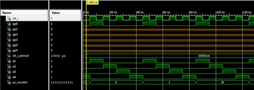
So as you can see I then run this up by first building a test bench file to generate the clock input and simulated. As you can see we have a perfect clock with Q1 and Q4 all in the right order and our pc_counter incrementing on each Q1 edge.
Adding the stack will be next time and is very simple as it's just two more signals declared the same as the pc_counter. However I’ll also look to generate the RAM and FLASH memory areas. The Flash should be easy to do but the RAM area has something we need to consider. It's not just simple RAM and needs to do something else, can you see what that is and how to resolve it?
- Comments
- Write a Comment Select to add a comment
m using spartan-2 xcs100 tq-144 series fpga kit..
i have to project so ???
To post reply to a comment, click on the 'reply' button attached to each comment. To post a new comment (not a reply to a comment) check out the 'Write a Comment' tab at the top of the comments.
Please login (on the right) if you already have an account on this platform.
Otherwise, please use this form to register (free) an join one of the largest online community for Electrical/Embedded/DSP/FPGA/ML engineers:


