


Homebrew CPUs: Messing around with a J1
In this article I will examine James Bowman's excellent J1 CPU; I will then proceed to mess around with various parts of it, making it smaller, more appropriate to my particular application, and possibly faster. I hope this will show you how easy it is to fiddle around with homemade CPUs and encourage you to make something weird and wonderful.
J1 CPU
My hat is off to James Bowman. J1 is pretty cool. It is a stack machine; it executes instructions in one cycle, it is small (~150 Spartan6 slices) and concise (<200 lines of Verilog). It features 16-bit instructions that directly control the CPU units, kind of like a VLIW CPU. The assembler can overlap sub-instructions whenever possible. Most common use of this is combining return with any non-branch-or-literal instruction – yes, you get a 0-cycle return most of the time. You can also modify stack pointers, write to memory or IO while performing an ALU operation.
J1 instruction encoding
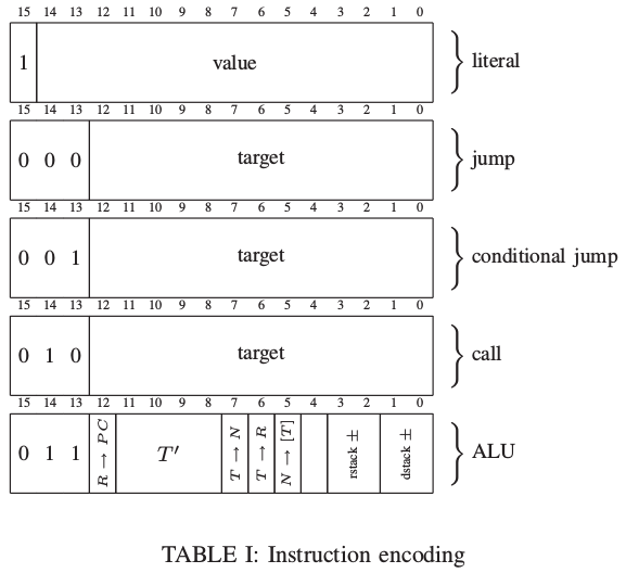
The instructions that start with 011 have bits dedicated to controlling the CPU units.
Bit 12, R->PC controls the PC mux: when it's 1, the next PC value comes from the top of the Return stack, making this instruction a Return in addition to anything else it does. Actually, to be a proper Return, the return stack needs to be decremented with bits 3:2 (J1 increments on push and decrements on pop).
Bits 11:8 marked T' control the loading of TOS, Top Of Stack register from the ALU. T->N forces TOS into NOS, or second-on-stack. T->R, similarly, forces TOS into the top of the return stack (don't forget to increment the RSTACK with bits 3:2). N->[T] initiates a memory write.
Those skilled in the stack arts will recognize the CPU as an FPGA-appropriate derivative of the Novix NC4016. More information on this chip is available in this chapter of the must-read book by Philip Koopman, Stack Computers: The New Wave. If you haven't read it, you really should. You'll be a hit at parties discussing why RISC is a gross misnomer in a world where stack machines still exist. If you still have doubts, look closely at the ARM instruction sets, and do your best to avoid vomiting.
It is pretty easy to map many primitive Forth operations to J1 instructions.

The evolution of the J1 CPU
James Bowman's github repo shows recent updates to the J1 processor. See the author's github repo.
Here are the highlights:
- The core is now parametrized for data width, and will synthesize at 16 or 32 bits!
- Memory-mapped IO has been replaced with an IO subsystem.
- The return bit has been moved to bit 7.
- The author recognized that there are few situations where a programmer wants to simultaneously write to memory and the IO ports and the return stack, and the new code uses 3 instruction bits to select the destination like this:
wire func_T_N = (insn[6:4] == 1); // TOS->NOS
wire func_T_R = (insn[6:4] == 2); // TOS->R
wire func_write = (insn[6:4] == 3); //TOS->MEM
wire func_iow = (insn[6:4] == 4);  //TOS->IO
The author's Verilog style has improved and is even more readable and enjoyable. The whole CPU now fits into 117 lines. Seriously look at it for yourself, it's worth the buttonclick. Beautiful, isn't it?
Debugging and testing the J1 processor
My workbench consists of a host Digilent S3 board with a Picoblaze CPU and a UART to communicate with my PC. There is also a target Xula2 Spartan 6 board that is controlled by the host. I can single-step or run a bunch of cycles on the target, and look at the target's registers on my pc via the Picoblaze monitor. More on my setup in another article.I was able to instantiate the J1 processor on my CPU workbench without any problems.My workbench clocks the target at 50MHz, and the CPU had no problems. The synthesis timing report indicated that the CPU could potentially run at 108MHz. Not bad.
I was not able to set up a Forth environment for it, as my Forth skills are rusty. But, I did build a simple J1 assembler in Common Lisp last week. Alas, it's for the old instruction set and I haven't updated it yet.
So, I hand-assembled a simple loop and stepped through it without problems. By the way, I use the Xilinx data2mem utility to patch the bitstream allowing me to re-assemble and reconfigure the FPGA almost instantly. If you are rebuilding your entire project from scratch you are making your life difficult for no good reason.
Improving and modifying the CPU
While the CPU is beautiful as is, it is tempting to make a few changes, just to see what happens. So here goes.
8'b011_?1001: st0N = st1 >> st0[4:0];
8'b011_?1010: st0N = st1 << st0[4:0];
Well, you may have heard people say that barrel shifters are large, and if you've seen one implemented, you would have to agree. Replacing these instructions with a more modest
8'b011_?1001: st0N = st1 >> 1;
8'b011_?1010: st0N = st1 << 1;
cuts the core size roughly in half (to 75 slices or so). I suppose sometimes it's really good to have a barrel shifter, but a minimal CPU that does not even have a subtract instruction (it is emulated with ~ +) probably does not shift enough to justify the size. Unless it does.
Anyway, I wanted to screw about with the ALU. The 21:1 mux smells a little funny, so I broke out the 4-bit ALU instruction decoder into a separate module. Changing the .xst file to keep the hierarchy, I should at least be able to see how big it is in the reports.
WTF, the Xilinx software is (still) a mess! Even changing the order of the ALU instructions within the module drastically affects the size of the module! What a drag! Keep hierarchy setting seems problematic - it seems that logic gets pushed into the top module somewhat randomly. Will have to investigate this at some point.
Anyway, there are way too many inputs into the ALU. How's about streamlinin' the ALU mux like this:
always @*
     case (sel[3:0])
       4'b0000: tos_res1 = tos;  //first 8 involve no nos
       4'b0001: tos_res1 = ~tos;
       4'b0010: tos_res1 = tos < nos;
       4'b0011: tos_res1 = (tos == nos);
       4'b0100: tos_res1 = tos<<1;
       4'b0101: tos_res1 = tos>>1;
       4'b0110: tos_res1 = {tos[14:0],tos[15]}; //rotate tos;
       4'b0111: tos_res1 = {tos[15:8]};
       4'b1000: tos_res1 = nos;
       4'b1001: tos_res1 = nos + tos;
       4'b1010: tos_res1 = nos - tos;
       4'b1011: tos_res1 = nos & tos;
       4'b1100: tos_res1 = nos | tos;
       4'b1101: tos_res1 = nos ^ tos;
       4'b1110: tos_res1 = tos+1;
       4'b1111: tos_res1 = tos-1;
     endcase // case (sel[3:0])
Now we are down to only two inputs – TOS, the top of the stack, and NOS, next on stack, and a clean
16:1 mux. (At least superficially - the shift operations introduce new input terms into the mux, so it's not a clean 16:1 mux anyway). This should make the ALU smaller, and we gain a minus instruction, rotate left, and inc/dec instructions.
How do we handle memory reads and IO reads? Ah, in front of the ALU we can place a 4-1 mux that decides what NOS (NOS is a bad name, but I don't feel like changing it now) should be. It can be the real NOS, or a memory port, or an IO port, or the return stack. Not a proper Forth behavior, but useful as all heck.
Now, in the spirit of being able to do many things at once, we've gained the ability to apply the ALU operation on the result of a memory read! You can decrement or AND the data from memory or the IO port for free.
Stacks
While I messing around, I dedicated the return stack for calls/returns only. That's right, there is no access to the RSTACK from my mangled CPU. Instead, there is a whole other stack, which I call ASTACK. Memory reads are issued from the top element of ASTACK (it's like Machine Forth's A register, except it's a stack too!). NOS is normally taken from DSTACK, but I use a free bit from the instruction to allow the CPU to use the ASTACK instead. Now, with two stacks, the automatic DUP from a literal and the automatic DROP for the conditional test don't make sense. Which stack do we use? DSTACK, I suppose. I wanted to experiment with not automatically dup/dropping. This changes the semantics a bit. It does simplify the stack pointer update logic.
I also changed the datastack increment bits to mean PUSH, POP. PUSH (which increments the stack) automatically causes a stack write. If both PUSH and POP are active, MEM_WRITE occurs. ASTACK similarly, controls IO_WRITE.
Speaking of stacks, I am using Spartan 6, and it should cost the same to have 32-deep stacks instead of 16-deep. So I widened the memory array to 32, and changed from [3:0] to [4:0] in a few places.
Wow, this is potent. Let's take stock of this new CPU:
- Two datastacks with one shared TOS register;
- Memory and IO reads enter the ALU and can be operated on during the same cycle.
The CPU synthesizes to approximately 76 slices, and timing report indicates that it may run at 128MHz. Whew!
Here is the new instruction set description:
1 xxx xxxx xxxx xxxx   literal
000 x xxxx xxxx xxxx   jump
001 x xxxx xxxx xxxx   cond
010 x xxxx xxxx xxxx   call
011:
12   : free
11-8 : alu instruction
7    : return
6-5  : 00 = dstack //NOS mux
       01 = astack
       10 = memory
       11 = io
4    : free
3    : apop  -- 11 means io-write
2    : apush /
1    : dpop   -- 11 means mem-write
0    : dpush  /
Not bad for a day's worth of fun. Now I wonder if I should've left the return stack access - I don't think I gain much by having it separated... The return stack can be used to do all kinds of tricks. Maybe I'll put it back later.
Man, it is even more painful to hand-assemble the test instructions. Well, it seems to work well enough. Do I like it? I don't know yet. I will have to go back and write a proper assembler in Common Lisp to really shake it down when I get a chance...
In the meantime, here is the code:j1hacked.v
I hope you are impressed with how easy it is to mess around with small CPUs. Much of this was made possible thanks to James Bowman's incredibly clean and simple design. It is not hard to understand everything about this CPU and make changes. Try the J1 CPU for yourself, and you may find modifying it to fit your needs actually enjoyable!
Jun 7 2015: added instruction decoding descriptions
- Comments
- Write a Comment Select to add a comment
To post reply to a comment, click on the 'reply' button attached to each comment. To post a new comment (not a reply to a comment) check out the 'Write a Comment' tab at the top of the comments.
Please login (on the right) if you already have an account on this platform.
Otherwise, please use this form to register (free) an join one of the largest online community for Electrical/Embedded/DSP/FPGA/ML engineers:


