


Feedback Controllers - Making Hardware with Firmware. Part 4. Engineering of Evaluation Hardware
- Part 1: Introduction
- Part 2: Ideal Model Examples
- Part 3: Sampled Data Aspects
- Part 4: Engineering of Evaluation Hardware (This Part)
- Part 5: Some FPGA Aspects
As ever, it should be noted that any examples shown may not necessarily be the best or most complete solution.
Project Context
Whilst this project has some of the characteristics of a commercial design engineering project, it also has a freedom more usually associated with a research project, albeit one with a strong application element.
The prime
objective for the hardware and the project as a whole is to produce a
high-quality design using modestly priced components, to allow
low-latency feedback controllers and arbitrary circuit emulators to be
developed and evaluated.
This article is a brief look at the
activities that went into the hardware side of the project along with
some observation and comment.
Elements of the Project Hardware Design
The following sequence of activities will be described.
- The Idea
- Objectives, Requirements, Specifications and Risk
- Block Diagrams
- The "Issue" Log
- Choosing Key Components/Devices
- Circuit Design, Due-Diligence and Engineering Tools
- PCB Design
- Purchasing
- Prototype Manufacture
- Preparing for Power-Up
- Discussion
1. The Idea
The concepts for the arbitrary circuit emulator and low-latency feedback controllers have been described in the previous parts of this series of articles. A MK I design for telecom test applications was done previously, and is shown below.
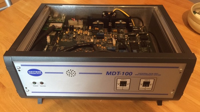
Fig 1. The Original MK I Arbitrary Circuit Emulator for Telecom Test Applications.
The current plan, is to produce a MK II design with a balance of modestly priced/state-of-the art electronics and to see what functionality and performance can be obtained not just for Arbitrary Circuit Emulators, but also for the low-latency feedback controllers that are an essential part of them.
2. Objectives, Requirements, Specifications and Risk
It was important to capture the project objectives, design requirements and unit specifications and also to identify any areas of project risk. These documents can be extensive for commercial, team-based projects, but for this personal research project, a simpler level was appropriate.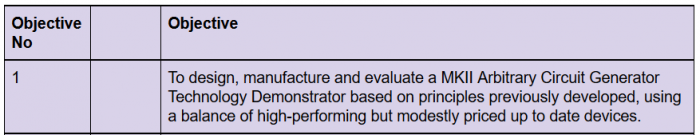
Fig 2. A simple statement of the first project objective.
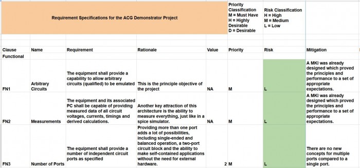
Fig 3. Example Requirements
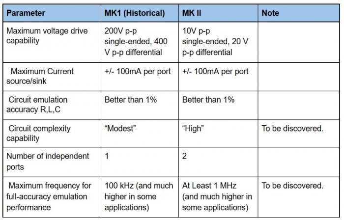
Fig 4. Indicative Specification
Living Documents - It was understood that "discoveries" and new influences would arise during the hardware design phase of the project that would affect the detail of the design and would inevitably require more time.
Risk Analysis - Given that all the key principles had already been proven in the MK I design and that the project was of an exploratory nature, there were no high risks envisaged. A medium, non-critical risk was simply the amount of time that might be needed.
3. Block Diagrams
Simple block diagrams were produced at the start of the project to encapsulate what was to be designed.
This is the 1st drawing for the design.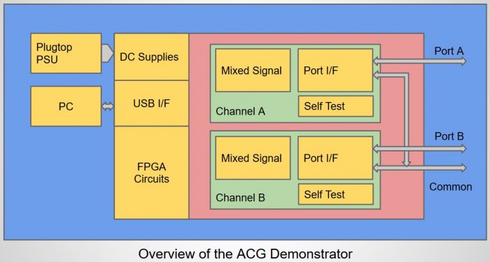
Fig 5. Basic concepts of the unit to be engineered
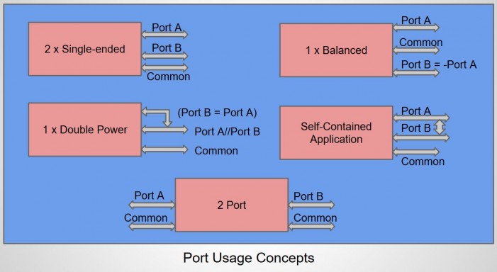
Fig 6. Port Usage - Arbitrary Circuit Emulator Mode
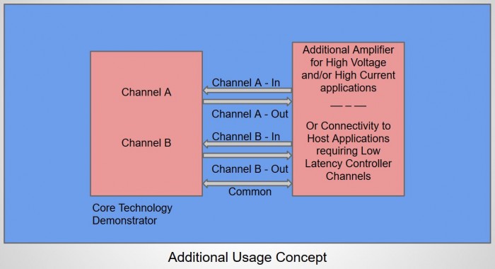
Fig 7. Port Usage - Arbitrary Circuit Boost Mode or Low-Latency Feedback Controller Mode
4. The "Issue" Log
An Issue log was created and proved invaluable for the capture of problems, unresolved issues and small doubts. It provided a great focus to ensure that the design was completed without any forgotten aspects.
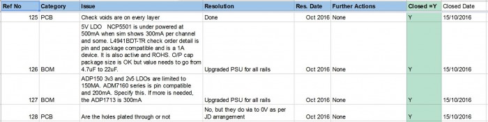
Fig 8. Some example issues from the issue log
5. Choosing Key Components/Devices
For the design of a technology evaluation unit, there is a clear desire
to choose only the highest performing components/devices available, but
in reality this has to be tempered by cost and other considerations.
Nonetheless, many of the components used are at the extremes of the
selection tables.
Among the complex factors that went into the optimized component choice, are :-
- Performance and functionality
- Cost
- Availability
- “Active” status, to avoid obsolescence issues
- “Green” issues such as ROHS compliance
- Ease of use
- Availability of CAD(Simulation) model
- Availability of CAD (PCB) model
- Familiarity (previous experience)
- Clarity of the data sheet and application notes
- Package size
- Package type
| Function |
Device(s) | Vendor(s) |
|---|---|---|
| Port Amplifier | THS3201-EP | TI |
| FPGA (Maths engine) | Cyclone V 5CEFA9F23C8N | INTEL/Altera |
| ADC | LTC2387- 16 or 18 bit | Linear Tech/ADI |
| ADC Driver | ADA4932 | ADI |
| DAC | LTC1668 | Linear Tech/ADI |
| Trim Amplifier |
VCA824 | TI |
| Wideband Op-amps |
MAX4227 , MAX4224 | Maxim |
| PhotoMos Relays | AQY221N2S | Omron and/or Panasonic |
| Relays | Series 103 | Pickering |
| Relay Drivers |
MAX6969 MAX4820 |
Maxim and TI |
| DC-DC convertors | 12Vdc to 5Vdc | Recom and Traco |
6. Circuit Design, Due-Diligence and Engineering Tools
The
Initial circuit design was based on experience, datasheet information
and innovation. But, it is the scope and power of modern simulation
tools that provides the degree of confidence that you need, to confirm
that the design does indeed function and perform as required and if not,
highlight the need to refine or redo the design or perhaps chose a
different device.
Spice Circuit Simulation
DC, AC, Transient and Noise simulations from a Spice simulator using vendor device models are an essential part of making a design that has a chance of working well, first time. Additional measurements of supply rail current can ensure that the power supply side of the design has enough capability.
The Spice simulation tools used were TI TINA and LTspice.
Here is a TI TINA example looking at a DAC drive circuit.
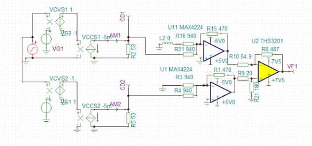
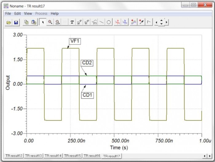
Fig 10. TI TINA Spice simulating DAC and amplifier drive levels and transient performance
FPGA Related
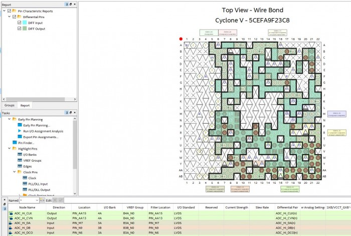
Fig 11. INTEL/Altera Quartus FPGA Pin Planner showing pins with differential signal capability
Circuit Schematic and Component Layout
The project used Altium Circuit Studio for the Schematic Design and Component Placement and although the design suite is of course capable of routing and pouring the copper on the PCB, this engineer is not inclined to get involved with that and the detailed tracking was outsourced.
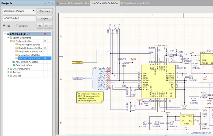
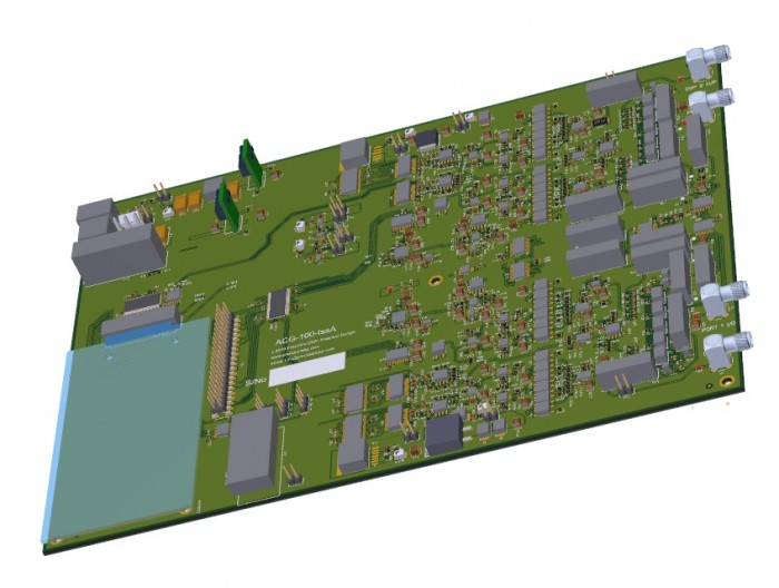
Fig 13. Altium Circuit Studio 3D View of the completed schematic design and component placement
7. PCB Design
PCB Layer Stack, Power Planes & Signal Integrity
Over the years, even the mixed-signal device specialists have changed their recommendations on ground plane strategy.
In seeking wisdom in this complex and sometimes contradictory field, I have found the analysis and writings of Henry Ott most helpful.
Ground Planes - I follow Henry Ott’s advice and construct multiple ground planes with carefully segregated regions and no splits, although there will be voids underneath high bandwidth components as per device datasheets.
PCB Layer Stack-Up - Again I am a fan of Henry Ott and his 8 layer stack-up has worked for me in the past. The concepts described in the link provided a starting point for the layer and plane usage in this project.
Signal Integrity - Requires careful attention to device data sheets, the use of controlled impedances where appropriate, great care in keeping incompatible signals separate and an awareness of how currents from DC upwards, flow through copper.
Thermal Considerations - Quite a few of the devices have thermal pads to dissipate heat into one or other of the PCB power planes. The device data sheets provide the sometimes intricate detail of preferred arrangements.
PCB track and plane routing - is outsourced. Apart from providing the guidance above, I leave it to a specialist.
PCB bare board manufacture - is outsourced.
8. Purchasing
Part of the original selection criteria for particular components was that where possible , a large stock was held by one of a few preferred distribution suppliers.
Identifying stock levels and pricing for the major distributors is easily done using Octopart or a similar service.
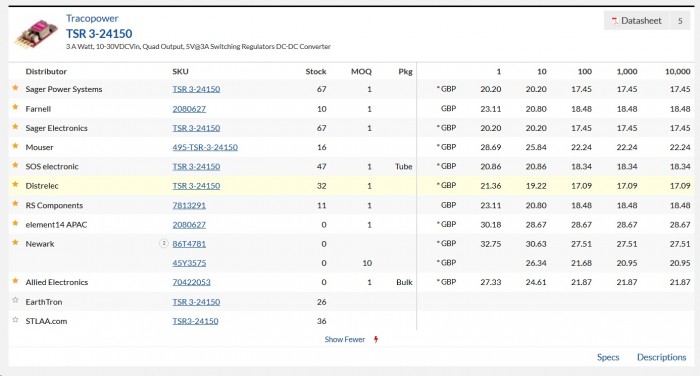
Fig 14. Example of an Octopart Search
Distribution suppliers used in the project include (in alphabetical order) :–
All of these have great searching and selection facilities and the speed at which orders are processed and delivered is a wonder to behold.
I have used the BOM upload facility with around 100 line items with Farnell and once the cogs had finished turning I received an updated list back with stock levels, pricing and a few multiple options to be resolved and then a 1 button click to add to the shopping basket.
This made the purchase of around 100 line items relatively quick and error free. I assume the other suppliers have the same facility, but I have not used those yet.
It seems that buying components is one of the easier tasks in the project.
9. Prototype Manufacture - is outsourced
Here is the 1st manufactured prototype.
_90083.jpg)
Fig 15. Manufactured PCB Assembly
10. Preparing for Power-Up
Power-up tests were done very carefully, in stages as follows :-
- Fit pillars, screws and washers
- Resistance to ground tests
- Brief application of power to monitor i/p current and check supply rail LED indicators
- Application of power and check current (using removable links) in the main supply rails
- Check no unduly high voltages on the pins that will connect to the FPGA or USB module
- Power down
- Fit the FPGA daughter card with spacers and washers and also the USB Module
- Power up and recheck currents in all major supply rails.
The picture below shows the complete unit with power applied.
_97224.jpg)
Fig 16. Fully Loaded PCB with power applied
11. Discussion
Here are a few comments about various aspects of the hardware design part of the project.
Design Discoveries
There were a number of issues that caused change or delay to the project. These were :-
- Additional system/hardware architecture was required to be developed to meet some of the notional specification items.
- A change of Schematic/PCB design software was needed due to the availability of PCB layout resources.
- A change of ADC device was made when a higher performance device was launched.
Mission Creep
There was a small amount of mission creep when it was decided to extend the functionality beyond the circuit emulation application to include the Feedback Controller Mode/External Boost Amplifier Mode.
Compromises
I don't think there have been any major compromises that affect the objectives. The design is probably over-engineered for a lot of applications. It feels about right for general research and when particular applications are considered later then maybe some appropriate refinements will come to light.
Here are the trade-offs that were applied :-
- Timescale - given the limited resources available, high-quality and lower project costs were favoured over speed of development.
- FPGA computing power - a lower cost floating-point centric Cyclone V FPGA was selected. This may prove to be the limiting factor for the maximum controller/circuit emulation complexity. But, the Cyclone 10 GX is on the near horizon and the possibility exists to re-engineer for an alternative FPGA daughter card.
- Power consumption - very little effort has gone into minimizing the circuit power. This is an area that can benefit from further design/innovation.
- Multiplexing the DACs - because the availability of FPGA pins was limited and to keep PCB complexity down, it was necessary to multiplex the 16bit DAC data to the DAC devices. This may or may not be a limiting factor. In any case, 1 of the channels can run without multiplexing to allow full-speed operation.
- Relays - some of the mechanical relays could have been replaced by smaller solid state OptoMos devices, but the cost would have been significantly increased.
Due-diligence
The availability of powerful Spice simulators and vendor device models means that really complex circuits can be modeled for real-world functionality and performance. A good deal of design effort was spent in confirming and/or optimizing the analogue circuit performance, using Spice simulation.
The use of the FPGA Quartus design suite to run trial compilations on FPGA pin allocation and signalling confirmed that the pin arrangements had the required functionality and that any constraints were met.
Defensive Design/Design for test
Defensive design can be used when there is some uncertainty and includes :-
- Providing resistors for pull-up/pull down rather than hard strapping to power rails
- Providing 0 ohm resistors on some op-amp o/ps to allow a small amount of resistance to be added in case of instability.
- Dual-PCB footprint to allow options on hard-to-source devices.
- Positions for compensation components which can be fitted if required
Design for test included a couple of items in addition to the built-in self-test and self-calibration. These were :-
- Provision of LED indicators on the main power rails
- Provision of links on the main power rails to allow current measurement
- Provision of a convenient Meter/Scope earthing point
Did the design work ?
The short answer is yes. For the tests conducted to date, the device connectivity, device operation and basic performance look good. The implementation of actual closed-loop DSP code is still to be done, but all the hardware around it looks ready to go.
OK, there was 1 design issue. The two DC-DC convertors that provide the +9V and-9V supplies are similar devices whose pin functions change depending on mode. That caused a bit of confusion on the schematic which required 1 resistor to be removed and another added on the back of the PCB.
Thank you for your interest.
Next up - Will be a look at FPGA and PC Programming Aspects
- Comments
- Write a Comment Select to add a comment
To post reply to a comment, click on the 'reply' button attached to each comment. To post a new comment (not a reply to a comment) check out the 'Write a Comment' tab at the top of the comments.
Please login (on the right) if you already have an account on this platform.
Otherwise, please use this form to register (free) an join one of the largest online community for Electrical/Embedded/DSP/FPGA/ML engineers:


