


Feedback Controllers - Making Hardware with Firmware. Part 5. Some FPGA Aspects.
- Part 5: Some FPGA Aspects (this part)
- Part 4: Engineering of Evaluation Hardware
- Part 3: Sampled Data Aspects
- Part 2: Ideal Model Examples
- Part 1: Introduction
As ever, it should be noted that any examples shown may not necessarily be the best or most complete solution.
FPGA Elements Considered in this Article
- Choice of FPGA - Cyclone V, Cyclone 10 GX
- Floating-Point Maths Capability
- Cost
- FPGA H/W Issues
- I/O standards 3V3 and 2V5, single-ended and differential signalling
- Termination Resistors
- Simultaneous switching
- Trial Compilation with all pins and technologies specified.
- Design methods
- Hierarchical Schematic
- Block Re-use
- VHDL
- Finite State Machine
- Vendor IP
- Random Logic
- For interest - Two recurring FPGA design questions/debates
- PC Connectivity
- Ethernet
- SPI
- UART
- Basic Floating-Point Maths Example
- Other FPGA Aspects
- Cyclone V FPGA, resources consumed to date
- Intel Quartus compile times
- IP Licences
1. Choice of FPGA - Cyclone V, Cyclone 10 GX
The original MKI Analogue Telecom Arbitrary Circuit Generator used an ADI ADSP-21161 device designed onto the main PCB as it's Maths engine.
Simply stated, the Maths engine requirements for the present MKII technology evaluation design were to :-
- Provide high-speed floating-point Maths operations
- Provide as many floating-point Maths resources as possible
- Have a modest cost
- Allow flexibility for alternative solutions
At the time of design, the optimum solution for the above was determined to be the Intel/Altera Cyclone V 5CEFA9F23C8N device fitted on the Arrow BeMicro CV A9 daughter card.
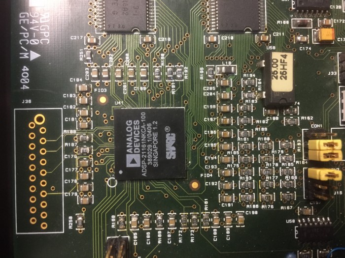
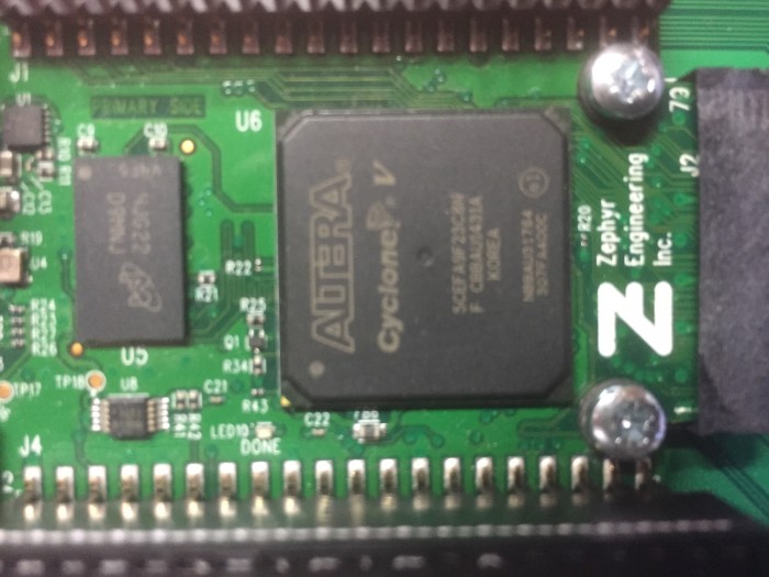
Fig 1. a) Historical Design ADI SHARC DSP b) Current design Intel/Altera Cyclone V
Here is a simplistic comparison of some headline parameters for the ADSP-21161 SHARC and the 5CEFA9F23C8N.
| Parameter | ADSP-21161 SHARC DSP | 5CEFA9F23C8N Cyclone V FPGA |
|---|---|---|
| Typical DSP Clock Speed | 100MHz | > 200MHz |
| DSP Resources | 2 Computation cores | 342 DSP Blocks |
| IEEE 32 bit Floating Point | Yes | Yes |
| Cost in low volume (Source Octopart 14 Nov 2017) | 47 USD Device only | 228 USD Device only 150 USD Device on BeMicro CV A9 |
Table 1. Simple comparison of some key device parameters
Performance expectation and DSP resources
This project was set out to see what performance could be achieved with a modestly priced floating-point FPGA. As such, there are no absolute values that must be achieved. But there is an expectation that the FPGA solution along with it's faster ADC's and other components should offer both higher-speed operation and provide for more complex DSP capability than the MKI design.
In rough terms let's say our expectation is for x 10 speed increase and x 10 DSP complexity increase.
To get more DSP work done we either need to do it faster or do more operations in parallel or both, so we can use (speed x resources) as a measure of capability. Without a detailed analysis, this can only be an order of magnitude guide as we need to see exactly how the SHARC cores compare with the FPGA DSP Blocks for the particular DSP tasks needed and even then we will see that there are major factors that affect the simple (speed x resources) model.
Simplistic View
SHARC capability (speed x resources) = 100 x 2 = 200
FPGA capability (speed x resources) = >200 x 342 = > 68400
FPGA/SHARC Capability = > 342 times or > 171 per controller channel. That looks good to meet our x 100 (speed x resources) expectation. BUT ...
Latency Delay - is important in feedback controller applications. Too much latency results in either poor or completely unstable closed-loop performance. Let's look at the Cycle Latency of the Cyclone V FPGA for a floating-point ADD operation.
| DSP Clock Frequency (MHz) | 300 | 200 | 100 | 50 | 25 |
| n = Cycle Latency for result | 36 | 14 | 6 | 2 | 1 |
| Latency (ns) | 120 | 70 | 60 | 40 | 40 |
| Logic Resources (LUTs) | 1637 | 999 | 835 | 736 | 697 |
Table 2. Latency for floating-point ADD reported by Quartus ALTERA_FP_FUNCTIONS wizard
Again, a detailed analysis of all the DSP operations including Multiply, Signed Integer(ADC)->Float and Float->Integer(DAC) would need to be considered to find the optimum DSP clock rate(s) but, it looks much more likely that our DSP clocks are going to be in the region of 50MHz rather than 200MHz or 300MHz for latency optimization.
Now our FPGA/SHARC Capability =(50x342)/(100x2) = 85.5 or 42.75 times per controller channel , which does not look so good for our x100 (speed x resources) expectation.
But, we do have some mitigating factors
- the SHARC also had to manage data capture and reporting whereas the FPGA DSP blocks do not
- some of the FPGA floating-point operations use general FPGA fabic and not DSP blocks
- we can split DSP operations into higher-priority and lower-priority latency operation
- Some DSP functions might be perfectly well served by fixed-point rather than floating-point maths
Comments
- The detailed design of the DSP algorithms and FPGA structures will require careful optimization effort if the x 100 (speed x complexity) expectation is to be achieved.
- The Cyclone 10 GX promises "2X Higher Performance for Up to Half the Cost" . The Cyclone 10 GX also provides more complex combined operations like multiply-accumulate which may help further with DSP efficiency, but it does have only 192 DSP Blocks (max) available.
The Main PCB allows for other FPGA solutions to be fitted. It could be that the Cyclone 10 GX or perhaps 1 off Cyclone 10 GX per channel is the optimum solution to achieve x 100 (speed x complexity) per channel of operation compared to the original MK I design.
2. FPGA H/W Issues
General
The Cyclone V FPGA is provided as part of the Arrow BeMicro CV A9 daughter card. As such, many of the FPGA and support chip hardware design issues are already covered. The downside to that is that the FPGA card specification was not absolutely ideal. In particular, the I/O voltage standards could not be mixed and additional level convertors were required on the main PCB. But, at around 150 USD for the card, the cost was lower than buying the FPGA device on its own.
Pin allocation and signalling standards
The devices on the main PCB that interface to the FPGA were a mix of 3V3 single-ended, 2V5 single-ended and 2V5 LVDS differential Tx and Rx signalling. The decision was made to set the BeMicro FPGA I/O levels to 2V5 for direct interface to the ADCs and then to provide 2V5 to 3V3 conversion for the other devices.
Not all FPGA I/O pins support all the standards so it is important to check for example, that the differential receive pairs that connect to the ADCs along with any desirable specialist resources like serializer/deserializer blocks are actually available on the pins allocated.
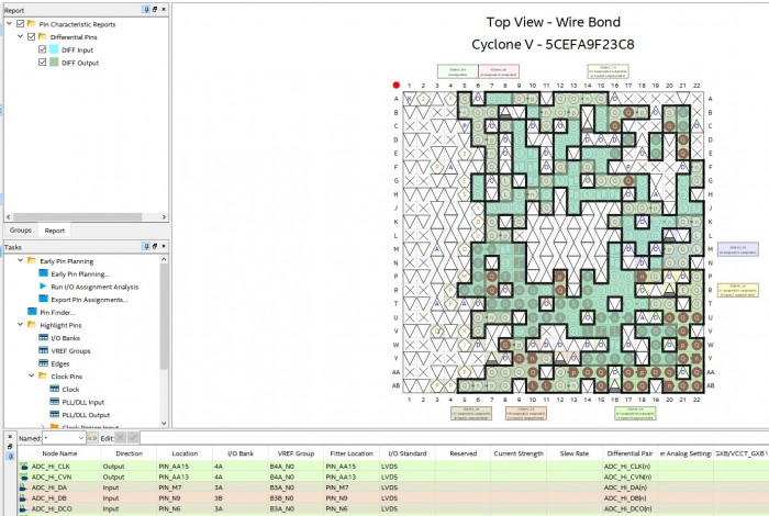
Fig 2. Quartus Pin Planner, showing pins that have differential Tx and Rx I/O capability
Termination Resistors
The differential LVDS signalling needed for the ADC signalling requires 100 ohm terminating resistances at both the ADC end and the FPGA end. The FPGA provides all the termination resistances required as internal components, but, the receiving FPGA termination must be explicitly enabled. This control is one of many pin options that is not obvious on the 1st level of design, but needs to be added from a sub-menu and then set.
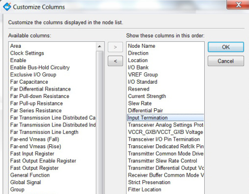
Fig 3. Adding the input termination option to the FPGA Pin settings
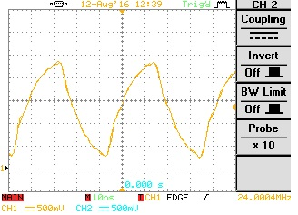
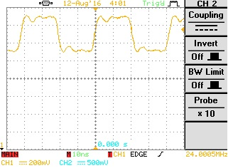
Note - scale is different between scope captures and scope earthing was not ideal.
Fig 4. a) LVDS signal without FPGA termination b) LVDS signal with Internal FPGA termination
Simultaneous switching
There are FPGA device rules for the allocation of pins which switch simultaneously. The easiest way to check that the requirements are met is to make a trial compilation with every pin defined for the signalling standard along with any pin options and pin operating frequency.
Trial Compilation
A trial compilation with all pins set to the required signalling standard with options and operating frequency will provide a report highlighting any issues. This will detect problems with pins not supporting a particular I/O standard and Simultaneous Switching Noise warnings etc.
3. FPGA Fabric Design Methods
My personal preference is for a Block Schematic design with :-
- Hierarchical levels to manage complexity
- Block re-use where possible for ease of maintenance
- FPGA coding by :-
- VHDL Code with Block representation
- Finite State Machines (FSM) with Block representation
- Vendor I/P Blocks
- Random Logic
Here is an example for a floating-point recursive oscillator.
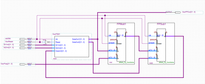
Fig 5. Example of a recursive Oscillator with Vendor IP, Random Logic and an FSM.
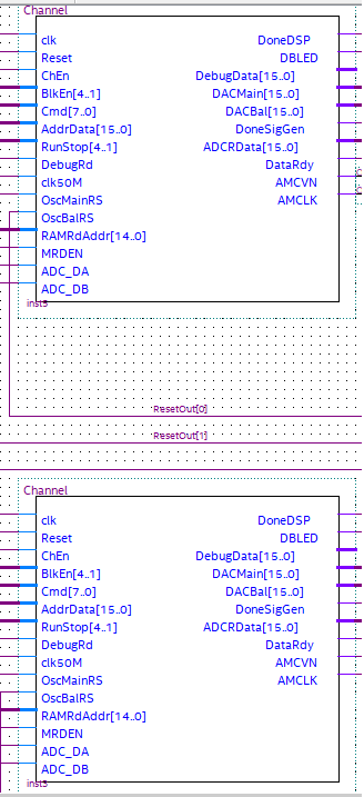
Block Reuse
Fig 6. Two Channels are just two copies of the same basic "Channel" design.
For interest - Two recurring FPGA design questions/debates
1. How many processes should my state machine use, 1, 2 or 3 ?
I have for some time opted for the single process solution by default and will continue to use that unless there is some critical situation that demands an extra process.
Xilinx Xcell issue 81, page 52 has a nice article by Adam Taylor about the subject.
2. When should I use Signals and when should I use Variables ?
The Xilinx coding style document includes the great comment that –
“Variables are commonly not understood and are therefore not used. Variables are also commonly used and not understood.”
As well as the discussion from the Xilinx coding document, the Book “Effective Coding with VHDL” by Ricardo Jasinski also has a good discussion and summary on the appropriate use of signals and variables.
4. PC Connectivity
Three options are available :-
- Ethernet - On the Bemicro daughter board. Not set-up or used yet
- USB to Fast SPI using an FTDI FT2232H device on a DLP USB1232H Module - Not set-up or used yet
- USB to UART using an FTDI FT2232H device on a DLP USB1232H Module - Low speed but easy to use for now.
Note - The UART for the FPGA was obtained from the OpenCores site.
5. Floating Point Maths Example
Floating Point Multiplication Example for the Intel/Altera Cyclone V FPGA using the Quartus Prime Lite Development Suite.
The circuit below consists of :-
- A Reset timer
- A Phase Locked Loop (PLL) generating a 100MHz clock (used) and a 200MHz clock (unused)
- A Finite State Machine (FSM) which generates 2 x signed 16 bit numbers
- 2 x signed integer to floating point convertors – designed for 100MHz, Latency 3 cycles
- A single precision floating -point multiplier – designed for 100MHz, Latency 3 cycles
- A floating-point to signed 16 bit convertor – designed for 100MHz, Latency 2 cycles
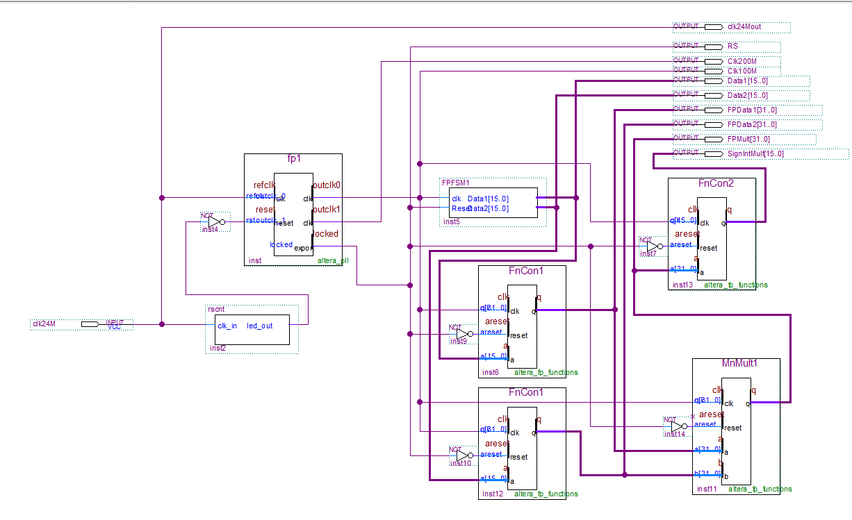
Fig 7. A simple Floating Point Mathematics Example.
The function of this circuit is to take two, signed 16 bit integers, convert them to floating-point, multiply them together and then convert the result back to a signed 16 bit integer.
Here is the simulation result
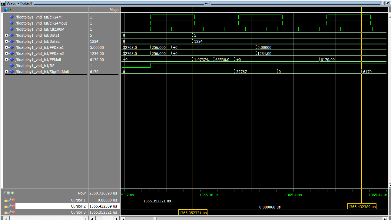
Fig 8. ModelSim Plot for the Floating-Point Mathematics Example
We can see the following :-
- The clock for this exercise is 100MHz
- The FSM generates the 16 bit integers 5 and 1234 at the left yellow cursor, 2 clock cycles after the reset is released (goes high)
- 3 clock cycles later, the floating-point numbers 5.00000 and 1234.00 appear at the output of the 16 bit signed integer to floating-point convertors
- 3 clock cycles after that the floating point number 6170.00 (= 5.00000 * 1234.00) appears at the output of the floating-point multiplier
- 2 clock cycles after that the signed integer number 6170 appears at the output of the floating-point to 16 bit signed integer convertor
Comments
- As predicted by the ALTERA_FP_FUNCTIONS wizard, the total latency from the arrival of the fixed-point i/p data (left cursor) to the appearance of the fixed-point result data (right cursor) is 3 + 3 + 2 = 8 clock cycles = 8 * 10ns = 80ns
- The relevance of this example to the practical hardware is that the unit uses 16 bit DACs and ADCs which operate with 16 bit integer signals. However we do require that the FPGA calculates the complex internal equations, using single-precision floating-point mathematics.
6. Other FPGA Aspects
Cyclone V FPGA, Resources Consumed
The FPGA project to date which does not yet include any significant DSP functionality for the Closed-Loop Controller functionality, uses the following FPGA resources :-
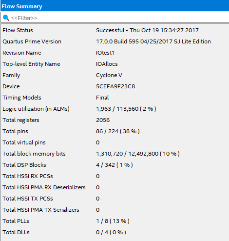
Fig 9. Cyclone V Resources used to date.
Intel Quartus compile times
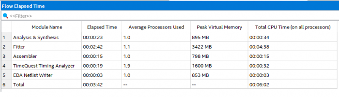
Fig 10. Quartus Compile times for the project - 3 Mins 42 Secs Total Elapsed Time
IP Licences
So far, all the required FPGA functionality has been achieved through a combination of original design, open-source code or free-to-use vendor IP.
The Intel/Altera Quartus design suite does provide and allow evaluation of licenced IP, for example a Numerically Controlled Oscillator (NCO) which runs whilst there is connectivity to the PC and continues to run for a limited timeout period after the PC link is removed.
Thank you for your interest.
Next up - Will be Calibration, Basic Measurements and Signal Generation- Comments
- Write a Comment Select to add a comment
To post reply to a comment, click on the 'reply' button attached to each comment. To post a new comment (not a reply to a comment) check out the 'Write a Comment' tab at the top of the comments.
Please login (on the right) if you already have an account on this platform.
Otherwise, please use this form to register (free) an join one of the largest online community for Electrical/Embedded/DSP/FPGA/ML engineers:


