


Feedback Controllers - Making Hardware with Firmware. Part 10. DSP/FPGAs Behaving Irrationally
This article will look at a design approach for feedback controllers
featuring low-latency "irrational" characteristics to enable the
creation of physical components such as transmission lines. Some thought
will also be given as to the capabilities of the currently utilized Intel Cyclone V, the new Cyclone 10 GX and the upcoming Xilinx
Versal floating-point FPGAs/ACAPs.
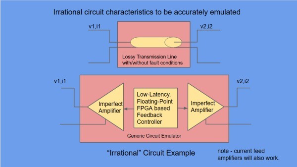
Fig 1. Making a Transmission Line, with the Circuit Emulator
Additional design notes will be published in due course, on the project website here and the latest developments can be followed on Twitter @precisiondsp. and LinkedIn
- Part 10: DSP/FPGAs Behaving Irrationally (this part)
- Part 9: Closing the low-latency loop
- Part 8: Control Loop Test-Bed
- Part 7: Turbo-charged Oscillators
- Part 6: Self-Calibration, Measurements and Signalling
- Part 5: Some FPGA Aspects
- Part 4: Engineering of Evaluation Hardware
- Part 3: Sampled Data Aspects
- Part 2: Ideal Model Examples
- Part 1: Introduction
As ever, it should be noted that any examples shown may not necessarily be the best or most complete solution.
Contents of this Article
- Motivation for Irrational Characteristics - Transmission Line
- A simple and powerful Transmission Line model
- a. Description of the model
- b. The RLGC Transmission Line Equations
- c. Spice simulation and selected validation results
- Approximating 1/Zo(s) and P(s) Irrational Characteristics
- a. A brute-force (but effective) approximation tool
- b. Simulations and validations
- i. MATLAB Zo(s) and P(s) approximation tests
- ii. Spice Transmission Line Tests
- MATLAB conversion of Zo(s) and P(s) to sample-data controllers
- a. Conversion of Zo(s) to a sampled data controller
- b. Potential Issues
- c. Potential Solutions
- Review of required/available FPGA Capability
- Discussion and Conclusions
1. Motivation for Irrational Characteristics - Transmission Line
In the last article, we successfully emulated a number of simple circuits based on a controller incorporating just a single Biquad filter. Now we would like to make something a bit more complicated.A Transmission Line offers some interesting new challenges as a circuit for emulation when compared to circuits made up of a simple collection of the basic Resistor, Inductor and Capacitor (RLC) components. In particular, the Laplace equations that describe the voltages and currents in the line, are irrational, non-integer powers of the Laplace operator s.
Examples of transmission lines are Coax cables and Copper Telephone/DSL cables. Wikipedia has a page describing a variety of types with applications and the science behind them.
A Transmission Line component is also offered as part of the LTSpice Spice simulator tool which allows the validation of designs against a proven reference model (with a little care). This component is known generally as the LTRA model.
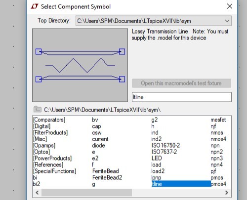
Fig 2. LTSpice has a Transmission Line component for testing ideas against a reference component
Laplace Transforms and Transfer Functions are a standard method of describing feedback control system elements such as those in the Circuit Emulator and they can also be used to describe both R,L,C type circuits and Transmission Line circuits, but whereas the R,L,C descriptions are rational (integer powers of the Laplace operator s), the Transmission Line descriptions are irrational (non-integer) powers of s and hence the title of this article.
The issues with that are :-
a) we are going to need to simplify the Transmission Line equations if we are going to use simple filtering to emulate them as we did for the RLC circuits.
b) Standard MATLAB does not handle irrational Transfer Functions.

Fig 3. Standard MATLAB throws an error for irrational powers of the Laplace operator s
So, to sum up - The the Transmission Line offers some interesting challenges and would be a useful component to add to the R,L,C capability of the Circuit Emulator. To get that working, we need to tackle Transmission Line Models and irrational Transfer Functions.
2. A simple and powerful Transmission Line model
a. Description of the model
The following model is a re-labeled and re-drawn version of similar arrangements that can now be seen in a number of books, academic papers, articles and blogs. For the record, I first saw this type of description in the book "Transmission Lines and Lumped Circuits", which was published in 2001.
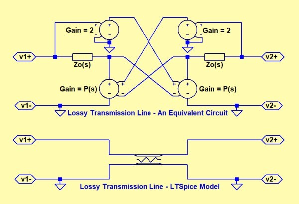
There are just 4 different circuit elements :-
- A simple voltage controlled voltage source with a gain of 2
- A differential voltage input, voltage source with a gain described by the Laplace Transform P(s).
- An Impedance described by the Laplace Transform Zo(s)
- 0V reference points.
Where s is the Laplace operator.
So,
all we need to do, to make our Lossy Transmission Line is perform some
simple maths, design filters providing transfer functions P(s) and
Zo(s) and then emulate the physical impedance of Zo(s).
b. The RLGC Transmission Line Equations (getting P(s) and Zo(s))
With reference to the standard literature, a Transmission Line may be described in terms of 5 quantities.
- R = the series resistance per unit length.
- L = the series inductance per unit length
- G = the parallel conductance per unit length
- C = the parallel capacitance per unit length
- X = the Length of the Line
In practical lines, R and L may vary significantly with frequency. Also, in some cases, C may be sensibly constant and G may be effectively = 0 and ignored.
Three expressions can be derived from the 5 parameters above which will link in to our model.
The Characteristic Impedance $$ Zo(s) =\sqrt \frac{ (R+Ls)} {(G+Cs)} $$
The Propagation Constant γ(s) (Greek lower case Gamma) $$ \gamma (s) =\sqrt {(R+Ls) (G+Cs)} $$and the Propagation Operator P(s) $$ P(s) = e^{- \gamma (s)X} $$
LTSpice provides us with a Laplace facility to create transfer functions such as Zo(s) and P(s) above and as it also has the Lossy Transmission line as a standard component we have everything we need to model and validate a Transmission Line Emulator.
c. Spice simulation and selected validation results
The following Parameters were chosen to provide a useful but not over-complex test case.
R = 400 ohms/km, L = 500uH/km, C = 50nF/km, G = 0 S/km, Mode = unbalanced (to match the basic LTSpice Model) and Length X = 1.1km for realistic tests and 1000km for Zo(s) verification.
At higher frequencies, Zo(s) will tend towards a value of 100 ohms resistive.
We are now in a position to build the complete model and try it with some test conditions.
Validation of the complete Spice Transmission Line ModelThe
purpose for the development of a Spice model made up of voltage
measurements, current generators and mathematical operations is not so
much to do with getting a good Spice simulation circuit, but more to do
with validating the fundamental block diagram for implementation by
FPGA.
Here is the Spice model used to validate the block diagram.
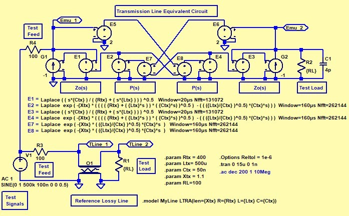
Fig 5. One of several possible models for the complete Transmission Line
A simpler version of Fig 5. was enough to produce perfect performance when comparing the frequency domain ac bode plot characteristics of the lower reference circuit and the upper emulation circuit. But, the results for the time domain transient responses were poor or useless and further enhancements were needed to get good result matching.
The transient analysis makes use of FFT's and Windows. I am not going to claim any great knowledge of the detail of these Spice FFT's and how they should be optimized. The Spice Help guidance says -
"The Laplace transform must be a function of s. The frequency response at
frequency f is found by substituting s with sqrt(-1)*2*pi*f. The time domain
behavior is found from the impulse response found from the Fourier transform of
the frequency domain response. LTspice must guess an appropriate frequency range
and resolution. The response must drop at high frequencies or an error is
reported. It is recommended that LTspice first be allowed to make a guess at
this and then check the accuracy by reducing reltol or explicitly setting nfft
and the window. The reciprocal of the value of the window is the frequency
resolution. The value of nfft times this resolution is the highest frequency
considered."
Briefly, the issues encountered and the adjustments made were :-
- General Accuracy - Improved by setting Reltol = 1e-6
- Zo(s) Performance - Improved by setting the Window and Nfft value for E1 and E3 as shown
- P(s) Performance - Improved by setting the Window and Nfft value for E2, E7, E8 and E4 as shown
- P(s) produced unwanted signal artifacts in advance of its delay characteristic - Fixed by splitting P(s) into 2 blocks, (P(s) - its ideal delay) E2 and E4 and ideal delay blocks E7 and E8.
- Instability with some load settings - added a small capacitor C1 at the Load side
Fig 5 shows a reference Transmission Line circuit using the LTSpice LTRA Lossy Line model and the proposed equivalent circuit. Both circuits are fed and loaded with identical signal and test components. The equivalent circuit uses a circuit emulator approach to produce the Zo(s) impedance, where the terminal voltage is measured (E1,E3) and the terminal current is controlled (G1,G2) by means of a feedback loop including a filter having the 1/Zo(s) characteristic (E1,E3). The P(s) filter is made up of E2 with E7 and E4 with E8. which gives better performance by splitting pure delay from the rest of the P(s) characteristic.
The Transmission Line R,L,C and length X characteristics and the RL Load settings are declared as parameters for ease of use and ensuring the reference and equivalent circuits are set to the same conditions. Either a .ac frequency response using a unit amplitude test signal or a .trans transient response using a unit amplitude 500kHz 1/2 cycle sine wave test signal can be selected.
Frequency Response Results
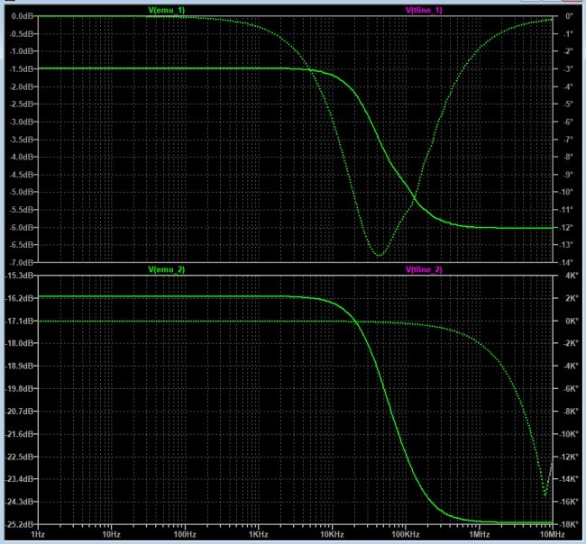
Fig 6. Emulation circuit and Reference input (Top) and Output (Bottom) frequency response results.
We are comparing the Emulation responses (green) with the reference responses (purple).
The
top traces are the input Bode plots. The bottom traces are the
respective output signal Bode plots for a load resistance RL of 100
ohms.
For the ac case, the input and output behaviors of the Transmission Line and the Circuit Emulator Model are identical.
Transient Response Results for RL = "Short circuit" (0.1ohm)
![]()
Fig 7. Emulation circuit and Reference input (Top and middle) and Output (Bottom) transient response results for RL = 0.1ohm
As before, we are comparing the Emulation responses (green) with the reference responses (purple).
The
top traces are the input time domain plots. The middle traces are input
detail and the bottom traces are the output time domain plots, all for
a "short circuit" load resistance RL of 0.1 ohms
Transient Response Results for RL = "Open circuit" (1Mohm)
![]()
Fig 8. Emulation circuit and Reference input (Top and middle) and Output (Bottom) transient response results for RL = 1Mohm
Again, we are comparing the Emulation responses (green) with the reference responses (purple).
The
top traces are the input time domain plots. The middle traces are input
detail and the bottom traces are the output time domain plots, all for
an "open circuit" load resistance RL of 1Mohms
Conclusions
The basic cross-coupled mathematical Transmission Line model with Impedance emulation looks good. It provides perfect agreement with the LTSpice LTRA Transmission Line component frequency response and very close agreement for a variety of transient responses. The Spice optimizations for the LTRA component and the Laplace calculations using FFT's and windows will not be considered further, as they are of no interest for the FPGA realization.
For
analysis purposes, It may be ok to wait a few seconds to get 15us worth
of transient response from a Spice simulation using FFTs, but in the
real-time feedback world we cannot afford to gather sample records and
perform FFTs. We need the Zo(s) and P(s) filter results at the earliest
opportunity after a new input sample value has arrived.
3. Approximating 1/Zo(s) and P(s) Irrational Characteristics
The Irrational Zo(s) (or 1/Zo(s)) and P(s) filter characteristics are not as easy to generate as the more familiar rational transfer functions. Base level MATLAB does not have the capability to handle non-integer transfer functions in s and Spice uses guesses and hand optimized FFTs with windows to convolve the filter impulse responses.
For an FPGA based solution utilizing single-precision floating-point arithmetic and requiring filter output values with minimum latency, we need something much much more efficient.
a. A brute-force (but effective) approximation tool
There may well be good mathematical/algorithm approaches available now, but when this problem was 1st considered, it was decided to use a simple iterative scheme to get a better and better fit to the reference response by adjusting the position of up to 8 poles and zeros. This was done at the time using a Scilab script and a Scilab GUI interface.
An example screenshot is shown below.
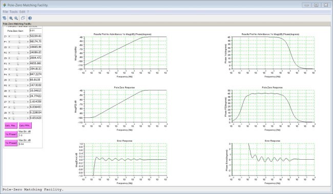
Fig 9. Scilab script and GUI for approximating irrational transfer functions by up to 8 poles and zeros
In this case the facility is matching the 1/Zo(s) characteristic and achieves a match of around +-0.1dB and +-0.5 degrees with 8 poles and zeros, over the frequency range of interest from 10Hz upwards.
b. Simulations and validations
The approximations obtained from the above utility were :-
| 1/Zo(s) | Gain = 0.01 | |||||||
| Zeros at | 3.282e05 , | 6.702e04 , | 1.259e04 , | 2229 , | 382.1 , | 63.12 , | 10.14 , | 1.433 |
| Poles at | 6.169e05 , | 1.514e05 , | 2.925e04 , | 5323 , | 929.4 , | 155.7 , | 25.36 , | 4.094 |
or we can simply invert to get Zo(s)
| Zo(s) | Gain = 100 | |||||||
| Zeros at | 6.169e05 , | 1.514e05 , | 2.925e04 , | 5323 , | 929.4 , | 155.7 , | 25.36 , | 4.094 |
| Poles at | 3.282e05 , | 6.702e04 , | 1.259e04 , | 2229 , | 382.1 , | 63.12 , | 10.14 , | 1.433 |
and P*(s) for a line length of 1.1km, where we only need 6 poles and zeros.
| P*(s) | Gain = 0.1108 | |||||||
| Zeros at | 6.61e05 , | 2.302e05 , | 4.573e04 , | 7910 , | 1159 , | 92.08 | ------- | ------- |
| Poles at | 3.616e05 , | 1.077e05 , | 2.925e04 , | 6312 , | 1043 , | 87.53 | ------- | ------- |
Note
- The P*(s) function approximated above is actually the Propagation
Operator P(s) with the pure time delay removed. The pure delay is easy
to create in an FPGA and the resulting P*(s) is a modestly simple
characteristic to implement.
These transfer functions were then evaluated
i. By comparing the above with the Zo(jw) and P*(jw) frequency responses of the fundamental R,L,G & C Transmission Line equations using MATLAB and
ii By comparing the complete Transmission Line Model with the Spice LTRA component using LTSpice.
i. MATLAB 1/Zo(s) and P*(s) approximation tests
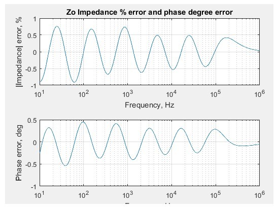
Fig 10. Plot of the Zo Impedance error w.r.t. Transmission Line R,L,G and C Equation.
It can be seen that the magnitude error is better than +-1% and the phase error is mostly better than +-0.5 degrees over the frequency range 10Hz to 1MHz.
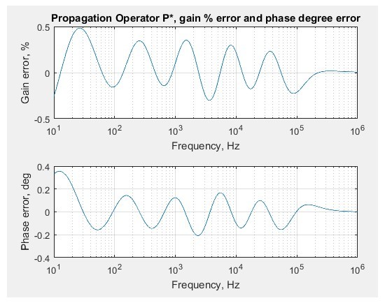
Fig 11. Plot of Propagation Operator P* error w.r.t. Transmission Line R,L,G and C Equation.
It can be seen that the magnitude error is better than +-0.5% and the phase error is mostly better than +-0.2 degrees over the frequency range 10Hz to 1MHz.
Conclusion
The
8 pole-zero model of Zo(s) and the 6 pole-zero model of P*(s) (for
1.1km line length) are looking like viable alternatives to the FFT based
Laplace models and LTRA component models used so far in the Spice
simulations.
ii. Spice Transmission Line Tests
We are now in a position to replace the FFT based Laplace functions in the Spice model with the 8 pole-zero approximation for Zo(s) and the 6 pole-zero approximation + a pure delay, for P(s). The pole-zero approximations were implemented by simple buffer-separated passive filters stages. These will be replaced by Biquad IIR filters in the FPGA version.
Here is an indication of the circuit detail, prior to reducing the filters into sub-circuits.
Fig 12. The complete Transmission Line and Reference LTRA Test Bed.
We
no longer have to worry about the fussy Laplace Window and Samples
settings and the need for a "stability capacitor" has gone.
A variety of validation tests were made for various test set-ups. In each case, a test voltage is applied to the test circuit and the reference LTRA reference component via 100 ohm resistors. Various waveform and load conditions were then applied, as detailed next.
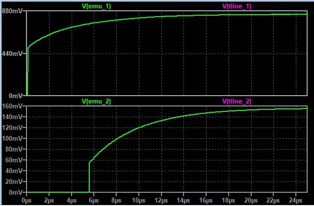
Fig 13. Step response of Test Circuit (Green) vs LTRA Component (Purple). Upper set are the Transmission Line inputs, Lower set are the outputs. 1V Voltage step, 100 ohm load.
V(emu_1) is the input of the proposed Transmission Line model, V(tline_1) is the input to the LTRA reference component.
V(emu_2) is the output of the proposed Transmission Line model, V(tline_2) is the output of the LTRA reference component.
Result - The Test Circuit vs the LTRA Component responses are the same for practical purposes.
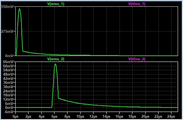
Fig
14. Pulse response of Test Circuit (Green) vs LTRA Component
(Purple). Upper set are the Transmission Line inputs, Lower set are the
outputs. 1V 500kHz half-cycle, 100 ohm load.
Result -The Test Circuit vs
the LTRA Component responses are the same for practical purposes.
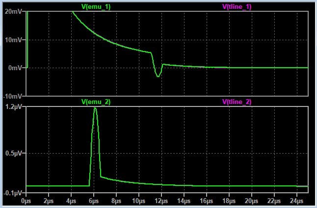
Fig 15. Short circuit pulse response of Test Circuit (Green) vs LTRA Component
(Purple). Upper set are the Transmission Line inputs (detail), Lower set are the outputs. 1V 500kHz half-cycle, 0.001 ohm load.
Result
- Here we can see the reflection at the line input due to the short
circuit at the line output. The Test Circuit vs the LTRA Component
responses are the same for practical purposes.
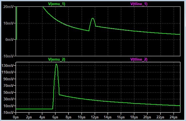
Fig 16. Open circuit pulse response of Test Circuit (Green) vs LTRA Component
(Purple). Upper set are the Transmission Line inputs (detail), Lower set are the outputs. 1V 500kHz half-cycle, 1M ohm load.
Result - Here
we can see the reflection at the line input due to the open circuit at
the line output. The Test Circuit vs the LTRA Component responses are
the same for practical purposes.
Conclusions The
8 pole-zero approximation of Zo(s) and 6 pole-zero + delay
approximation to P(s) provides excellent performance matching to the
LTRA Transmission Line component, without the tuning and stability
issues associated with the Spice Laplace FFT based functions.
Just as importantly, it offers the possibility of creating the Zo(s) and P(s) filters using a single-precision floating-point FPGA with Biquad filter implementations.
4. MATLAB conversion of Zo(s) and P(s) to sample-data controllers
Having validated the Transmission Line model and the irrational Zo(s) and P(s) approximations, we can now look at manipulating the Zo(s) and P(s) models in MATLAB and deriving digital controllers suitable for realization by an FPGA.
We actually have a number of choices of controller for the emulation of Zo(s). One of these is to measure current and multiply by Zo(s) to generate the appropriate voltage, another is to measure voltage and multiply by 1/Zo(s) to generate the appropriate current.
We will now look at the Zo(s) option for conversion to a digital controller Zo(z)
As the concepts for conversion of P(s) to P(z) are the same, there is no need to detail that.
a. Conversion of Zo(s) to a sampled data controller
It is worth noting a comment by MATLAB - “Working with TF and ZPK models often results in high-order polynomials whose evaluation can be plagued by inaccuracies.”
I mention that because in the course of manipulating s and z domain transfer functions and making multiple de-compositions and re-compositions I have indeed seen equivalent models lose accuracy, to the point that they become useless. For that reason I try to keep transformations to a minimum.
One starting point is to take the Zo(s) 8 pole-zero model in 4 pairs and convert each pair into a 2nd order digital filter using the first-order hold method at a sample rate of 8Msps. We can then confirm the frequency response match between the 8 pole-zero model transfer function (TF) and the digital filter TF.
This is part of the code for that
% These are the base equations for Zo manipulation
%
%Zc = [ -Z1 -Z2 -Z3 -Z4 -Z5 -Z6 -Z7 -Z8 ]; % 8 Zeros from matching utility
%Pc = [ -P1 -P2 -P3 -P4 -P5 -P6 -P7 -P8 ]; % 8 poles from matching utility
%Kc is the gain for Zo(s) = 100
%Gsys = zpk(Zc,Pc,Kc);                     % ZPK form

PairAZeros = [ -Z1 -Z2 ];                % 1st pair of zeros
PairAPoles = [ -P1 -P2 ];                % 1st pair of poles
PairAs = zpk(PairAZeros,PairAPoles,1);   % s domain 2 poles, 2 zeros
PairAz = c2d(PairAs,(1/Fs),'foh');       % discretise at 8Msps

PairBZeros = [ -Z3 -Z4 ];                % 2nd pair of zeros
PairBPoles = [ -P3 -P4 ];                % 2nd pair of poles
PairBs = zpk(PairBZeros,PairBPoles,1);   % s domain 2 poles, 2 zeros
PairBz = c2d(PairBs,(1/Fs),'foh');       % discretise at 8Msps

PairCZeros = [ -Z5 -Z6 ];                % 3rd pair of zeros
PairCPoles = [ -P5 -P6 ];                % 3rd pair of poles
PairCs = zpk(PairCZeros,PairCPoles,1);   % s domain 2 poles, 2 zeros
PairCz = c2d(PairCs,(1/Fs),'foh');       % discretise at 8Msps

PairDZeros = [ -Z7 -Z8 ];                % 4th pair of zeros
PairDPoles = [ -P7 -P8 ];                % 4th pair of poles
PairDs = zpk(PairDZeros,PairDPoles,1);   % s domain 2 poles, 2 zeros
PairDz = c2d(PairDs,(1/Fs),'foh');       % discretise at 8Msps

Pairss = Kc*PairAs*PairBs*PairCs*PairDs; % s domain 4 pole-zero pairs
Pairsz = Kc*PairAz*PairBz*PairCz*PairDz; % z domain 4 pole-zero pairs
                                         % Kc is the Zo filtergain = 100
figure(7);
bodeplot(Gsys,Pairss,Pairsz,w,opts);     % show the resulting curves
grid on  % grid on
and the resulting plot
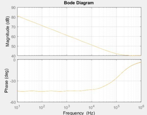
Fig 17. Comparing Zo - 8 pole-zero model, 4 x pole-zero pair model and digital filter model
Result - The 3 models are sensibly equivalent.
b. Potential Issues
One
area of concern is whether the models are hiding characteristics that
work in the near-perfect world of double-precision arithmetic but would
fail in a single-precision floating-point FPGA implementation.
Such
a situation can easily occur when a Biquad filter is operating at a
high sample rate but is required to produce a low frequency
characteristic. In such a case we see the Biquad coefficients get very
close to 1, to the point where single-precision arithmetic does not have
sufficient resolution to create the required filter. This can lead not
just to inaccurate results, but also to unstable responses.
The Highest frequency second order digital filter PairAz is reported ny MATLAB as :-
1.0231 (z-0.9812) (z-0.9258)
PairAz = ----------------------------
(z-0.9917) (z-0.9598)
Sample time: 1.25e-07 seconds
Discrete-time zero/pole/gain model.
Which looks OK.
But, the Lowest frequency second order digital filter PairDz is reported by MATLAB as :-
1
PairDz = -------
(z-1)^2
Sample time: 1.25e-07 seconds
Discrete-time zero/pole/gain model.
Which looks ill-conditioned.
If however you cut and paste the PairDz denominator values into "notepad", you get poles more accurately reported as :-
[0.999999820902531;0.999998732086996]
Which
might be tough to achieve with single precision arithmetic, given the
several additions and multiplications needed in a Biquad.
c. Potential Solutions
If the above filter cannot be achieved satisfactorily with single-precision FPGA arithmetic, some options to improve the situation are :-
- Reduce the sample rate for the entire digital filter, if the resulting performance is acceptable
- Remove the low frequency poles and zeros, if the resulting performance is acceptable
- Factor out the low frequency problem filter section and run that section at a lower rate than the rest of the filter.
The last option looks favorite as we can maintain the high sample rate for most of the filter and we don't have to lose any of the low frequency poles and zeros in the Zo approximation model.
One approach is to represent the 4 cascaded filter sections as a partial fraction (PF) sum. The problem low-frequency section(s) can then be redesigned at a lower sample rate whilst the higher frequency sections can be bundled back into a cascaded section running at the full sample rate.
Whilst there may be a requirement for additional anti-alias filtering on the lower sample rate section(s), it may also be possible drive them from part way along the high sample-rate chain where some filtering may already have been performed.
In short there are lots of ways that filter sections operating at different sample rates can be combined. That along with other aspects such as pole-zero ordering and specific Biquad implementation form will be left for another time.
Example of "Mix and Match" Cascade and PF forms with MATLAB
Our s domain Zo Model in MATLAB is :-
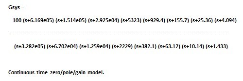
i.e. a gain of 100 and 8 poles and zeros
We can decompose that into Gseg1,2,3,4,& 5 with the following part code
% Cascade vs Sum vs Mix of Sections Example
[num,den] = tfdata(Gsys,'v');             % extract the Numerator and Denominator
[numres,denres,kres] = residue(num,den);  % get the partial fraction form
[Zseg1,Pseg1] = residue(numres(1:2),denres(1:2),0); % Poles/Zeros Segment1
[Zseg2,Pseg2] = residue(numres(3:4),denres(3:4),0); % Poles/Zeros Segment2
[Zseg3,Pseg3] = residue(numres(5:6),denres(5:6),0); % Poles/Zeros Segment3
[Zseg4,Pseg4] = residue(numres(7:8),denres(7:8),0); % Poles/Zeros Segment4

% convert to sys forms
Gseg1 = tf(Zseg1,Pseg1); %Transfer Function Segment1
Gseg2 = tf(Zseg2,Pseg2); %Transfer Function Segment2
Gseg3 = tf(Zseg3,Pseg3); %Transfer Function Segment3
Gseg4 = tf(Zseg4,Pseg4); %Transfer Function Segment4
Gseg5 = kres ;           %The Gain part

Gsum = (Gseg1 + Gseg2 + Gseg3 + Gseg4 + Gseg5); %

figure(8);
bodeplot(Gsys,Gsum,w,opts);     % show the resulting curve
grid on  % grid on
That includes a check that the sum of the decomposed segments is equal to the original Gsys, which it is.
Gseg4 is our potentially troublesome filter with the low frequency characteristic
$$ Gseg4 = \frac{ 2.745e05 s + 1.308e06}{s^2 + 11.58 s + 14.53} $$
We can now bundle the rest of the segments back up into cascade form with the following part code and deal with the Gseg4 sample rate as separate issue.
% bundle segments 1,2&3 and gain together
[Zseg123,Pseg123] = residue(numres(1:6),denres(1:6),kres); % Poles/Zeros Segments1,2,3 & gain
Gseg123 = tf(Zseg123,Pseg123); %Transfer Function Segment1,2,3 & gain
Gsum2 = Gseg123 + Gseg4;

figure(9);
bodeplot(Gsys,Gsum2,w,opts);     % show the resulting curve
grid on  % grid on
and again we check that the cascade/sum combo matches the original Gsys, which it does.
In diagram form the operations were :-
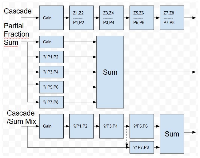
Fig 18. Unbundling and re-bundling filter segments to allow problem parts to be dealt with separately e.g. different sample rates for the two paths to the lower Sum block.
Conclusions
The basic conversion of the Zo(s) controller to an equivalent digital
controller Zo(z) is simple. But, because the controller operates over a
wide bandwidth, the lower frequency segments become ill-conditioned for
an 8Msps sample rate and single precision arithmetic. Factoring out the
troublesome segment and utilizing a mixed cascade/sum arrangement is
being considered to allow a lower sample rate for the problem filter.
Additional
implementation aspects such as Biquad type e.g. Transposed Direct Form
II and Pole-Zero ordering will need to be considered along with the
already proven compensations for ADC, Computation and DAC reconstruction
delays.
5. Review of required/available FPGA Capability
It is yet to be proven as to whether the INTEL Cyclone V 5CEFA9F23C8N in conjunction with the ADI/LinearTech LTC2387-16 SAR ADC and LTC1668 DAC are able to perform fast enough to run the controllers and mixed-signal electronics necessary for the Transmission Line emulation. Compensation methods can account for delays due to anti-alias filters, ADC conversion, Control-law calculation and DAC reconstruction, but there are limits to that.
At present, the biggest contribution to unwanted controller delays is the Cyclone V FPGA at around 125ns. The ADC is next at around 104ns. Options for lower latency components are available for both the FPGA and the ADC although an alternative ADC may come at the cost of poorer signal to noise performance.
Here is a rough review of how selected floating-point DSP(historical) and FPGAs are looking for low-latency number-crunching, in terms of floating-point operations per second * 10^9 (GFLOPs).
NB
- This IS a rough guide not all comparisons are exact or known for
actual real-world performance in the context of closed-loop controllers.
| Biggest Device in Family | No of DSPs | Total GFLOPs | GFLOPs/DSP | Comments |
|---|---|---|---|---|
| ADSP-21161 | 2 | 0.44 | 0.22 | Used in a historical design |
| Cyclone V | 342 | ---- | 0.269 | Based on floating-point multiply with a latency of 6 cycles. Aimed at low cost. |
| Cyclone V | 342 | ---- | 0.048 | Based on floating-point multiply with optimized latency. Aimed at low cost. |
| Cyclone 10 GX | 192 | 173 | 0.9 | Peak figure. Optimized latency example has been proven by Quartus design and simulation suite, to be at least 6 x better than Cyclone V. Aimed at low cost. |
| Xilinx Versal Prime | 3080 | 5000 | 1.62 | Peak Figure. New product. Unknown conditions, latency etc. Cost ? |
| Xilinx Versal AI Core | 400 "AI Engines" | 8000 | 20 | Peak Figure. New product. Unknown conditions, latency etc. Cost ? |
| Xilinx Versal AI Core | 1968 "DSP Engines" | 3200 | 1.62 | Peak Figure. New product. Unknown conditions, latency etc. Cost ? |
Table 1. A simplistic look at some some selected floating-point performance figures.
The above calculations are rather basic and we may be comparing different high/mid/low end device/pricing sectors but, it is interesting to see the "value for money" INTEL Cyclone offerings and the upcoming unknown price offerings from Xilinx.
For now, the INTEL Cyclone 10 GX is still looking good as a replacement for the Cyclone V, to achieve lower-latency higher-throughput arithmetic as and when needed. It does have fewer DSPs than the Cyclone V, but that is more than compensated for by the faster performance for this application.
The Xilinx Versal adaptive compute acceleration platform (ACAP) is one to watch.
Conclusion
The
Cyclone V FPGA may have the capability to do the floating-point
arithmetic for the Transmission Line Emulation, but if not, then the
Cyclone 10 GX is looking good to provide the horsepower needed.
GFLOPs/DSP/£,$,€,¥ etc. driven by the AI boom is looking fascinating.
6. Discussion and Conclusions
Having successfully emulated a number of simple circuits last time, this article has shown how the significantly more complex and irrational behavior of a basic lossy transmission line can be modeled and approximated to a high degree of accuracy such that the digital controllers needed for circuit emulation can be implemented in a floating-point FPGA. A previously published transmission line model and a pragmatic approximation method form the basis of an efficient mathematical model which has been validated against the Spice standard LTRA component.
One minor issue which has been seen is a loss of
high accuracy at very low frequencies e.g. 10Hz, if the Zo(s)
approximation is restricted to 8 poles and zeros. Adding additional
poles and zeros will extend the accuracy in that region. In any case,
the Zo(s) impedance is high at this point so its influence on signal
voltages and currents is minimal anyway.
Some practical implementation issues have been considered and potential solutions discussed. Should the need for lower-latency higher-throughput mathematics be needed, then an FPGA upgrade to the Cyclone 10 GX looks to be appropriate. After that, the spotlight falls on the ADC to gain further speed/latency improvements.
Some development has already
been undertaken to extend the complexity of the emulation to include the
frequency dependent R,L,G,C line characteristics to account for the
"skin effect" in a transmission line. Also, the ideas developed can be
used for a single port transmission line with distant-end loading and/or
faults at various distances emulated by additional digital filter
stages.
Conclusions
By using appropriate models, approximations and proven architecture it
is seen as feasible, to realize the irrational controllers needed to
allow a basic two-port transmission line to be fully emulated utilizing a
floating-point FPGA to provide the required mathematics.
The practical implementation is yet to be made and tested and may need an upgrade to a lower-latency FPGA than the present Cyclone V.
Thank you for your interest, Steve Twitter @precisiondsp. and LinkedIn
- Comments
- Write a Comment Select to add a comment
To post reply to a comment, click on the 'reply' button attached to each comment. To post a new comment (not a reply to a comment) check out the 'Write a Comment' tab at the top of the comments.
Please login (on the right) if you already have an account on this platform.
Otherwise, please use this form to register (free) an join one of the largest online community for Electrical/Embedded/DSP/FPGA/ML engineers:


