


Part 11. Using -ve Latency DSP to Cancel Unwanted Delays in Sampled-Data Filters/Controllers
Some applications demand zero-latency or zero unwanted latency signal processing. Negative latency DSP may sound like the stuff of science fiction or broken physics but the arrangement as described has been successfully implemented in both commercial and research projects.
Please note
that active Intellectual Property applies to these concepts, if you are
interested in that aspect, more information can be found here.
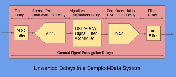
Fig 1. Unwanted Delays associated with a Sampled-Data System
This series of articles has described an instrumentation project in all its technical aspects from concept, feedback control structures, technology selection, hardware design, floating-point FPGA/DSP algorithm development, built-in signal generation, measurement & self-test, PC GUI design for initialization, operation and analysis to approaches for some exotic irrational transfer function synthesis.The objective of updating an original Analog Devices Sharc design to a faster, more capable floating-point Intel Cyclone V FPGA design has been achieved and many innovations added, especially in the self-test/analysis area.
If you would like to discuss any of the issues covered in the series, I can be reached at steve.maslen@btinternet.com or LinkedIn
- Part 11: Using -ve Latency DSP to Cancel Unwanted Delays (this final part)
- Part 10 DSP/FPGAs Behaving Irrationally
- Part 9: Closing the low-latency loop
- Part 8: Control Loop Test-Bed
- Part 7: Turbo-charged Oscillators
- Part 6: Self-Calibration, Measurements and Signalling
- Part 5: Some FPGA Aspects
- Part 4: Engineering of Evaluation Hardware
- Part 3: Sampled Data Aspects
- Part 2: Ideal Model Examples
- Part 1: Introduction
As ever, it should be noted that any examples shown may not necessarily be the best or most complete solution.
Contents of this Article
- Motivation for Avoiding Sampled-Data System Delays
- Sources of Unwanted Delay in Sampled-Data Systems
- Designing a Zero-Latency Signal Processing Capability
- Developing a -ve Latency DSP Block
- Incorporating the -ve Latency DSP Block into a Sampled-Data System
- An illustrative example
- Comparing Gs with Gz MATLAB and Simulink Responses
- Comparing Gs with G b0+DF3 Simulink Responses
- -ve and Zero-Latency Discussion and Conclusions
- Overall Project Discussion and Conclusions
1. Motivation for Avoiding Sampled-Data System Delays
Fig 1 shows the basic elements that make up a typical Sampled-Data system. These are :-
- An analogue to digital convertor (ADC) and associated input filter
- A maths-capable processor such as a DSP device or an FPGA
- A digital to analogue convertor (DAC) and associated output filter
This arrangement provides a means to take an electronic signal, apply complex processing to it and then provide the result as another electronic signal for use elsewhere.
In addition to the signal delays due to the desired, complex processing, there will be other delays that are due to the practical operation of the ADC, DSP/FPGA and DAC devices.
In modern devices, these delays may be in the order
of 100's ns in total, which in an application like open loop audio
processing may be negligible. However there are some applications like
high-frequency closed-loop control, where a 100ns delay is completely
unacceptable. If we consider an example where we require a precision
DSP/FPGA generated characteristic at 1MHz in a closed-loop scenario,
then a delay of 100ns represents an unwanted phase shift of 36° which will certainly result in poor performance and may result in completely unstable behavior.
For the application described in this series of articles and others perhaps from the world of experimental physics, we require not just low latency, but complex signal processing with no significant unwanted latency.
2. Sources of Unwanted Delay in Sampled-Data Systems
As indicated in Fig 1, there are unwanted delays due to :-
- General circuit, signal-propagation time
- Filters
- ADC
- DAC
- DSP/FPGA Calculation time
Note - Some ADC vendors have made statements such as "No-Latency 18-bit 15Msps SAR ADC Improves Performance in High-Speed Control and Data Acquisition Applications" This does not actually mean zero time delay from sample-point to data-available but rather zero pipeline cycle delays over and above the basic ADC sample and conversion operation.
The most significant unwanted delay contributors in this project application are :-
| Source of Delay | Description | Typical value |
|---|---|---|
| ADC LTC2387- 16 | Delay from the sample point until the ADC data is available | 90ns |
| DSP/FPGA Cyclone V | Time taken to perform the processing calculations | 125ns |
| DAC Mux | Time to apply calculated values to DAC multiplexors | 40ns |
| DAC LTC1668 | Time taken for the output to appear, after the DAC is "fired" | 10ns |
| DAC | The so called Zero Order Hold (ZOH) effect | Sample Period/2 |
We need an arrangement that can cancel out these and other unwanted delays whilst retaining the capability to provide complex and precise signal processing characteristics.
3. Designing a Zero-Latency Signal Processing Capability
This description will cover a basic-level generic arrangement as originally described in the Patent submission here.
Since then, further developments have been added to provide
substantially higher bandwidth performance. These new developments have
been implemented and proven on the current development test-bed hardware
and an upgrade of ADC and FPGA will allow further substantial
improvements.
This is probably a good point to make a couple of definitions. In the context of this project, the following are defined :-
"Zero-Latency Signal Processing" - Signal processing that exhibits negligible unwanted time delay and in some cases negligible absolute time delay. Negligible in this context, typically means delays of < 15ns.
"Negative (-ve) Latency DSP"
- a Digital Filter that produces a desired characteristic with output
values that are available earlier than for its basic form and earlier
than required.
In describing generic Digital Filters (DF), there are a number of equivalent representations and sign conventions as well as decompositions of higher-order filters into second-order blocks to provide a better behaved solution for implementation by limited-resolution maths hardware. Some MATLAB example representations can be seen here.
In the following descriptions, a Direct Form, Type II format will be used for an nth order filter using standard MATLAB symbols notation. The reader can transform these to a preferred format, if desired.
We will start by developing a -ve latency DSP block and then see how that can be used to build a zero-latency signal processing capability.
a. Developing a -ve Latency DSP Block
The starting point is a standard format nth order filter representation as follows :-
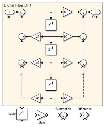
Fig 2. Generic nth order Digital Filter DF1 described using standard MATLAB blocks
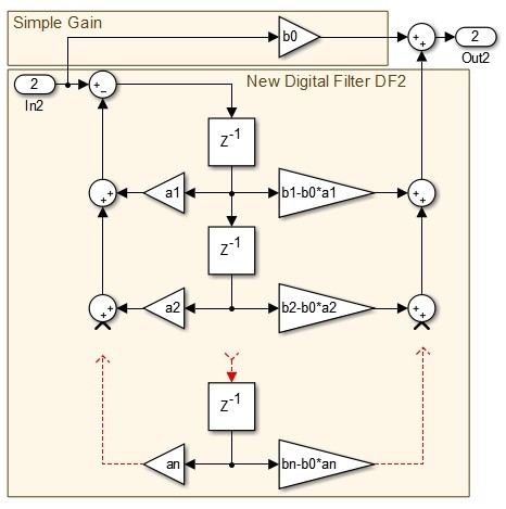
Fig 3. A Filter b0 + DF2 which is equivalent to DF1
For the moment, we will ignore the separated simple gain b0. For the remaining DF2 we can shift all the output gains b1-b0*a1 etc. up one delay tap to get a new filter DF3 :-
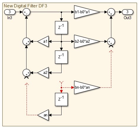
Fig 4. The Digital Filter DF3 which is as DF2 but with the output signal 1 sample too early (-ve latency)
In summary, we have split the original Digital Filter into 2 parts. The first part is a simple gain b0. The second part is a new Digital Filter DF3 which contains all the elements that define the required complex frequency dependent characteristics. Importantly, the DF3 characteristic produces the required samples 1 sample too soon.
b. Incorporating the -ve Latency DSP Block into a Sampled-Data System
Fig 1 can now redrawn with the new b0 , DF3 arrangement as :-
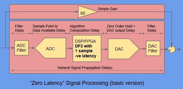
The remaining task is to ensure that the total of all the sampled-data system delays is equal to the DF3 negative latency advance. If the 1 sample advance is too much, just add some more signal delay in the DSP/FPGA.
The b0 simple gain path can be designed with a high-bandwidth variable gain amplifier with care taken to ensure that the layout results in minimal end to end propagation delay. Additional high frequency shaping can be added as appropriate.
This combination can provide complex Digital Filtering with an unwanted latency of just a few ns in the simple gain path and negligible unwanted latency contribution in the DSP path at frequencies approaching Nyquist. The DF3, b0 design values can be obtained from a simple MATLAB continuous s domain to z domain "c2d" conversion plus another line of code to factor out b0 and apply the tap shift. The unwanted latency effects of the ADC acquisition delay, DSP/FPGA computation delay, DAC ZOH and output delay and filter delays no longer spoil the the conversion for practical applications.
4. An Illustrative Example
To
illustrate the techniques, a classic PID Controller was chosen for no
other reason than it is a simple transfer function with enough dynamics
to make it interesting. The reference transfer function in the s domain
is (MATLAB Style) :-
1e-09 s^2 + 7e-05 s + 1
Gs = -----------------------
1e-10 s^2 + 5e-05 s
It
is transformed to the z domain with 2Msps sample rate using the MATLAB
C2D function with the method chosen as "foh" or first order hold.
9.01 z^2 - 17.71 z + 8.7
Gz = ------------------------
z^2 - 1.779 z + 0.7788
Sample time: 5e-07 seconds
Actually, those numbers are rounded for display purposes by MATLAB
The value for the simple gain part is b0 = 9.00964
The values for the DF3 digital filter are calculated using :-
DF3= (Gz - b0)*z; % Factor out b0 and shift up the o/p taps
Various results were then taken for Gs, Gz and G b0 , DF3 as follows.
a. Comparing Gs with Gz MATLAB and Simulink Responses
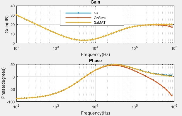
Fig 6. Plots for a PID controller
Gs (blue) is the s domain continuous reference plot
GzMAT(yellow) is an equivalent z domain plot using the MATLAB c2d function with method = "foh" and sample rate = 2Msps.
GzSimu(red) is a time domain derived plot using a Simulink model of Gz.
As discussed in Part 3 of this series the MATLAB bode plot only considers the values at the sampling instances. To get a bode plot for a real-world sampled-data system with a DAC and associated Zero Order Hold, we need something else. A rather inefficient Simulink model is currently used for that and the GzSimu curve is the result.
In summary, the GzMAT curves are a
very good approximation to the reference Gs curves, but are not
realizable by a simple sampled-data system. The GzSimu curves are
produced by the Gz transfer function with a DAC for reconstruction. The
Gain curve falls off by around 3dB and the phase curve falls off by
around 75 ° near the Nyquist
point. This is not usable for a high-precision application which needs
negligible unwanted latency and we have not even taken into account the
other delays due to ADC conversion and Digital Filter computation time
etc. , which will add to the poor performance.
b. Comparing Gs and G b0 , DF3 Simulink Responses
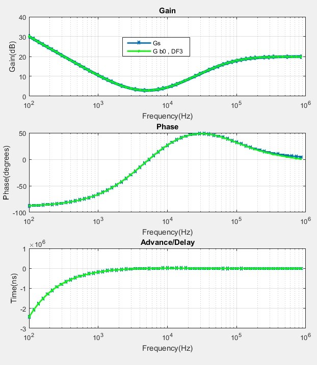
Fig 7. Plots for a PID controller, reference and the b0 , DF3 "Zero Unwanted Latency" Scheme
Gs (blue) is the s domain continuous reference plot
G b0 , DF3 is the "Zero Unwanted Latency" scheme described previously.
The results for the G b0 , DF3
system correspond well to the reference curves and the small errors
approaching the Nyquist point can be further improved by the
incorporation a 1st order ZOH correction filter along with the DF3
implementation. In fact, the high frequency performance gets even better
beyond the DF3 Nyquist point, as it is dependent only on the b0 gain
(with additional shaping if wanted). But care must be taken to avoid any
spurious alias contributions from DF3.
Practical hardware test-bed results for a number of transfer functions have been presented in Part 9 of the series.
5. -ve and Zero Latency Discussion and Conclusions
As stated at the beginning, there are some applications that demand signal processing with negligible unwanted latency.
A
Digital Filter can provide near ideal characteristics, but only at the
instantaneous sample points. Practical, physical, sampled-data systems
can produce the required Digital Filter characteristics but they also
incur delays due to ADC data-available latency, DSP/FPGA computation
time, Zero Order Hold and other DAC delays and additional filter and
signal propagation delays.
This article has described the basic version of an arrangement that can create the near ideal Digital Filter characteristics without those unwanted delays. This arrangement has been proven and used in commercial and research projects.
The basic version concept is based on a Digital Filter that provides its output values 1 sample earlier than required (-ve latency DSP) such that the other unwanted sampled-data delays can be cancelled out. This Digital Filter is then combined with a simple gain (with frequency shaping if wanted), to result in a signal processing arrangement that provides the precision characteristic required, without significant unwanted latency "Zero Latency signal-processing".
The maximum
bandwidth of operation now has to be considered in 2 parts. the gain
with optional shaping is the limiting factor at high frequencies and is
only limited by the devices used. The present TI VCA824
device has a 0.1dB Gain Flatness to 135 MHz. The sampled-data part is
limited by ADC, DSP/FPGA computaion, DAC and other delays. The present
basic version hardware can operate at a sample rate of around 2Msps. An
enhanced version using the same hardware will probably improve to around
4Msps. An upgrade of ADC and FPGA (Cyclone 10 GX) is anticipated to move the sample rate into the 10's Msps, with high frequency characteristics > 100MHz. The Xilinx Versal devices perhaps have the potential to provide substantial additional performance.
Conclusions
A solid basis for signal processing without unwanted latency has been presented and proven in practice for real-world applications. Extensions to the basic arrangement have been developed to provide enhanced performance. Further substantial improvements are envisaged with an upgrade to key Mixed-Signal and FPGA devices.
The original patent
arrangement was developed because the closed-loop circuit emulator
required it. I assume that other demanding applications may yet come to
light.
6. Overall Project Discussion and Conclusions
This project was conceived to combine many of my technical interests into a single project and to present the various facets of an electronics engineering project from conception to working system to anyone that might be interested in some or all of its aspects.
The original circuit emulator application was based round an Analog Devices Sharc DSP and operated at a sample-rate of 200ksps. The current design uses an Intel Cyclone V FPGA and operates at 2Msps with option for around 4Msps. A Cyclone 10 GX and associated upgrades may move the sample-rate up to 20Msps and so we progress. Of course, the FPGAs also have the benefit of massively concurrent operation to provide vastly increased complexity over the original dual-core DSP.
As with any project there are joys, surprises and bumps in the road.
Some less desirable aspects were :-
- It took much longer than desired
- Changing Schematic/PCB CAD package part way through
- Frying a section of circuit when probing a sensitive signal pin adjacent to a power rail
- Ending up with more spurious port capacitance than wanted despite being careful during the design ( although, even that turned out to be removable with the help of DSP )
- Disappointment that the Cyclone V floating-point maths latency is so high
Plus side
- Innovations for improving floating-point DSP oscillators
- Innovations for extending the basic "Zero-latency signal-processing" arrangements
- Developing an efficient Gain/Phase/Latency, high-resolution frequency response measurement system
- Making it all work
- Helpful vendors providing samples and technical support
Next steps ?
Having proved all the basics with a selection of simple transfer
functions, the next step might be to develop multiple and more complex
transfer functions and to optimize the FPGA operation for faster sample
rates. Applications requiring irrational transfer function filters are
very appealing. But, my feeling is that the Cyclone V is near its maths
latency limit and a lot of energy would go into meeting the set-up and
hold constraints within the FPGA for more complex examples.
The reality is that an FPGA upgrade is due, to enable serious performance gains and to make life simpler. Fast 1 or 2 cycle high clock-rate floating-point mathematics is needed and the Cyclone V does not have that.
It would also be nice to explore the high-level synthesis of DSP on an
FPGA using Intel's DSP builder or similar. In applications where
latency is critical it would be interesting to see if a compiler can
produce designs with latency characteristics as low as hand-crafted
ones.
In the short-term, the enhanced architectures/MATLAB activities for "Zero-latency signal-processing" need to be properly documented, so that is where any effort will go.
ConclusionsIt
was fun (mostly). The future looks very bright for the DSP applications
and FPGA engineering, with some great recently released devices
and new devices appearing on the horizon. We will be able to crunch
numbers ever faster and more of them at the same time.
I hope that at least some of it was of interest to the DSP, FPGA & Electronics communities.
Again,
If you would like to discuss any of the issues covered in the series, I
can be reached at steve.maslen@btinternet.com and LinkedIn
Many thanks to Stephane Boucher and DSP, FPGA & Electronics Related for hosting these articles.
- Comments
- Write a Comment Select to add a comment

Steve, I have few "dumb" questions:
[1] In your text associated with your Figure 7 you used the phrase "G b0+DF3." I'm assuming that the phrase "G b0+DF3" is the name you have assigned to some kind of digital filter. If my assumption is correct is it possible for you to give us that "G b0+DF3" filter's block diagram and tell us what are the coefficients you used in that block diagram to produce your Figure 7 curves?
[2] In the caption for Figure 7 you used the phrase "b0+DF3." What is "b0+DF3"? Is it a digital filter? How is "b0+DF3" related to this thing you call "G b0+DF3"?
[3] In the bottom panel of your Figure 7 you present a curve you call "Advance/Delay" associated with what I think(?) is a digital filter that you call "G b0+DF3". If "G b0+DF3" is indeed a digital filter, how is Figure 7's "Advance/Delay" curve related to what is traditionally called the "group delay" of the "G b0+DF3" filter?
Sorry for all the questions Steve. Again, your blog is very interesting. I'm merely trying to figure out if your "Zero Unwanted Latency" scheme can be used to reduce the time delay (the "group delay") of a simple IIR lowpass filter.
Thanks,
[-Rick-]

Hi Rick, Thank you for the comments. I'll work out a MATLAB script to clarify and post it later. Cheers, Steve
Hi Rick, I hope the following code will clarify the situation. My working code had a different legacy notation so I reworked it without the Simulink stuff and hopefully without bugs :-)
[1] & [2] It starts with a reference transfer function/filter Gs
DF1 is a z domain equivalent transfer function/filter
b0 is the uppermost DF1 filter output side coefficient as per Fig 2.
DF2 is the DF1 filter - b0 like you see in Fig 3.
DF3 is the DF2 filter with output taps advanced 1 sample as Fig 4
The value of gain b0 and the DF3 characteristics are then passed to a Simulink Model which works out the Bode plot from time-domain data. The Simulink model also includes a time delay representing the ADC and Computation time plus an implicit Zero Order Hold representing a DAC output.
I prefer Simulink as I can see exactly what is going on moment by moment and compare with my Oscilloscope traces from the real hardware.
You can run the code and get all the coefficient values.
[3] For my purposes, Advance/Delay is a simple conversion of phase to time delay at each frequency e.g. -36 ° at 1MHz is -36/(360*10^6) = -100ns, a delay.
If you wish, I can probably provide more efficient feedback by email at steve.maslen@btinternet.com
All the best, Steve
opts = bodeoptions('cstprefs');  % declare options for bode plot
opts.FreqUnits = 'Hz';           % change the bode options to Hz

s = tf('s');                     % declare the s operator

% Reference transfer function
Gs = (1e-09*s^2 + 7e-05*s + 1)/(1e-10*s^2 + 5e-05*s);

z = zpk('z',0.0000005);           % declare the z operator
DF1 = c2d(Gs,0.0000005,'foh');    % discretise at 2Msps
% zoh,foh,impulse,tustin,matched  - method options avaiable

[num,den,Ts] = tfdata(DF1,'v'); % get the numerator and denominator of DF1

%factoring out the DF1 b0 term to get DF2
b0 = num(1);                % get b0 for analogue gain
DF2 = (DF1 - b0);           % factor out b0 from DF1
DF3 = DF2*z;                % shift up the o/p taps to get DF3
[num2,den2,Ts] = tfdata(DF3,'v');
% then we poke the gain b0 and num2,den2 which define DF3 into Simulink
% Simulink then works out the Bode plot of b0 + DF3 from time-domain data

bode(Gs,DF1,opts)           % Bode plots of the Gs reference and DF1
grid on  % grid on
Hi Steve. Thanks for the code. As I wrote, I don't have MATLAB's Control Toolbox so I'm not able to run your code.
Steve, please have a look at the following diagrams.

Let's say I have the 2nd-order IIR filter as shown in my above Figure A. Is my above Figure B the correct implementation of your "Zero Unwanted Latency" scheme applied to my Figure A filter?
As I wrote before, I'm trying to figure out what is the block diagram of the filter that implements your "Zero Unwanted Latency" scheme. I want to know if your "Zero Unwanted Latency" scheme can be used to reduce the time delay
(the "group delay") of a simple IIR lowpass filter.
Thanks!
[-Rick-]
Hi Rick, your Fig B above is not quite the implementation for my situation. It's like this :-

Fig C
Where, in the lower path, the sum of the unwanted delays = the time advance inherent in DF3. Your Fig B does not include the lower path delays, that I needed to cancel. The upper path is the gain b0.
Implementing b0 + DF3 as defined in my code above will produce something different to my principle objective.
I don't recall what MATLAB without toolboxes can and can't do for digital filters, so here is all the b0 and DF3 information, in basic terms from the MATLAB console
Fig C. Upper Path b0 = 9.009644937052249
Fig C. Lower Path (DF3 part)
-1.681 z (z-1.001)
DF3 = ------------------ sample rate = 2Msps
(z-1) (z-0.7788)
in higher resolution form
DF3 Numerator -1.68098947377311 1.68320146594239 0
DF3 Denominator 1 -1.77880078307141 0.778800783071405
To simulate Fig C for my example, you then need to include the DAC ZOH characteristic and a time delay of 250ns representing the ADC, Computation and other delays, in the lower path. The smaller effects of the ADC and DAC filter amplitude responses are ignored in the example, to highlight the primary principle.
Cheers, Steve
Hi Steve. Thanks for the additional information. I will continue experimenting.
[-Rick-]
Rick, I see that I created a source of confusion by referring to the final arrangement as "b0+DF3" which implied output = input * (b0+DF3).
In my mind I meant b0 with DF3 as per the arrangement shown in Fig 5.
I have changed the notations from "b0+DF3" to "b0 , DF3" to indicate that. Everything else stays the same. Cheers, Steve
I have been alerted that I may have mixed some sign conventions (I mentioned it as a source of confusion :-). I'll check when I get back onto it next week.
Update - All looks to be OK.

Hi Steve,
Thanks for the blog.
I have modeled your idea as below:
###################################
x = randn(1,1024);
b0 = 0.1; b1 = .376; b2 = -.71;
a0 = 1; a1 = -.7; a2 = .72;
y1 = filter([b0,b1,b2],[a0,a1,a2],x);
y2 = filter([b1-b0*a1,b2-b0*a2,0],[a0,a1,a2],x);
y2 = x*b0 + [0 y2(1:end-1)];
plot(y1,'.-');hold;
plot(y2,'g.--');
#######################
Your upper and lower branch seem to be just equivalent to original filter. I can't see any advance. am I doing something wrong?
Regards
Kaz
Hi Kaz,
Thanks for the comment and the code.
I hope what you showed, is that it did work.
If I understand what you did, then
y1 = filter([b0,b1,b2],[a0,a1,a2],x); % is my DF1,the desired response
y2 = filter([b1-b0*a1,b2-b0*a2,0],[a0,a1,a2],x); % is my DF3
at this stage DF3 is producing samples 1 sample too soon, but the unwanted delays due to ADC, Computation and DAC ZOH + any padding needed are producing an unwanted delay of 1 sample. The net effect is for the advance of DF3 to cancel the unwanted + padding delays to end up with the desired filter in spite of all the latency that usually spoils it.
you then redefine y2
y2 = x*b0 + [0 y2(1:end-1)];
in which [0 y2(1:end-1)] adds a 1 sample delay representing the unwanted latency discussed above.
your unwanted 1 sample delay + 1 sample advance due to DF3 = 0 unwanted latency, as desired.
Regards, Steve
Hi Steve. I believe kaz's June 25th code demonstrates that the blog's Figure 2 network is equivalent to the blog's Figure 3 network.
Thanks Steve,
So basically you want to offset the chain delay (assumed to be one sample) rather than the filter group delay.
The idea doesn't look clear to me. Because if (DF1) output is identical sample by sample to (DF3+upper branch) then I might just use DF1 to get same output and avoid new DF3 filter and its upper branch.
I believe you are thinking this way:
I have a given filter and some delay in the chain. I want to cancel the chain delay so will modify filter to get advance(less groupdelay and different response) and add outer branch. This yes will cancel out the delay and give equivalent net filtering but your original filter's groupdelay will stay unchanged.
Regards
Kaz
Hi Kaz,
"The idea doesn't look clear to me.
Because if (DF1) output is identical sample by sample to (DF3+upper
branch) then I might just use DF1 to get same output and avoid new DF3
filter and its upper branch."
In my applications, I start with a desired filter response, normally defined in the continuous domain. I then use MATLAB to get a digital filter version of that = DF1, and the responses align nicely, but only at the sample points.
If I make a practical sampled-data system ADC+DF1+DAC the result is poor or useless because of the delays added by the ADC, Calculation time and DAC ZOH.
By factoring out b0 as a simple gain and then implementing the sample-data system with a DF3 designed to cancel out the unwanted delays, I achieve the desired result in a practically realizable solution.
The key issue for me is that a practical DF1 filter made with an ADC, a DF1 computer and a DAC does not produce an usable response. By using the arrangement discussed, we can achieve a response that is usable in an instrumentation grade application.
Regards, Steve
P.S. I just absorbed the second part of your comment. Yes, my prime objective is take a defined filter characteristic and make it realizable by use of DSP without incurring the usual unwanted effects due to latency. I have not looked at taking a defined filter and tried to make it into something different.
Thanks Steve,
Understood.
The main point of confusion may arise if someone assumes you can also cancel out the desired filter's own delay(groupdelay). I don't see that happening in my model since you get same DF1 response at the end from DF3+upper branch. But yes your modified filter (DF3+upper branch) can be designed to cancel out external delay (external to filter).
Kaz
Kaz,
Thank you for opening up some interesting philosophical points and I confirm that the current work has been concerned with cancelling the ADC, Computation, DAC reconstruction and other associated delays that spoil the practical implementation of a given filter and not with taking a given filter and improving its characteristics.
Steve
Hi Steve. Your blog has intrigued me enough that I've been studying what happens when we convert the below traditional Figure A 2nd-order IIR filter into the below Figure B 2nd-order IIR filter. What I've learned is both interesting and surprising.

I'm currently studying the conversion of 1st- and 3rd-order IIR filters. I hope to write a blog describing what I've learned.
Hi Rick, I'll look out for that. It's good that we can still find the unexpected at a modestly fundamental level.
Thanks
To post reply to a comment, click on the 'reply' button attached to each comment. To post a new comment (not a reply to a comment) check out the 'Write a Comment' tab at the top of the comments.
Please login (on the right) if you already have an account on this platform.
Otherwise, please use this form to register (free) an join one of the largest online community for Electrical/Embedded/DSP/FPGA/ML engineers:


