


Use DPLL to Lock Digital Oscillator to 1PPS Signal
Introduction
There are occasions where it is desirable to lock a digital oscillator to an external time reference such as the 1PPS (One Pulse Per Second) signal output from a GPS receiver. One approach would be to synchronize a fixed frequency oscillator on the leading edge of the 1PPS signal. In many cases, this will result in adequate performance. However, in situations where simple synchronization does not provide adequate performance, digital phase-lock techniques can be applied to a digital oscillator to achieve much better results.
This article will describe a DPLL that locks a digital oscillator, i.e. a Direct Digital Synthesizer (DDS), to an external 1PPS timing reference and which can achieve time alignment with GPS to better than 1 microsecond. The DPLL also removes the frequency error of the DDS reference oscillator, and can maintain time lock in the event that the external 1PPS timing reference is removed. Furthermore, the DPLL will smoothly re-lock to the external timing reference when it is restored.
This article will not provide an in-depth review of phase-lock techniques. The Web has many excellent articles on the subject. FPGARelated.com blogger Reza Ameli published an excellent introductory article on the subject of Discrete-time (or Digital) Phase-Locked Loops (DPLLs). Readers not familiar with phase-lock techniques are encouraged to read his article: Discrete-time PLLs, Part 1: Basics.
Problem Description
In my work, I need to be able to operate equipment in such a manner that it is aligned to an external timing reference such as the GPS 1PPS signal. This requirement is generally associated with a requirement to provide time tags for measurements of events in a consistent manner even when the equipment is distributed on a network. The resolution required of the time tags that accompany the measurements is generally such that normal time synchronization methods, such as Network Time Protocol (NTP), are inadequate for the purpose.
Every oscillator made has a fundamental error: its absolute frequency with respect to its specified operating frequency is non-zero. Furthermore, even if its frequency was absolutely correct, its phase relative to another oscillator at the same frequency would not likely be the same.
To reliably exchange data between two systems operating using different clocks, the frequencies have to be the same or there will exist a finite probability that the data will arrive within the meta-stability window of the receiver and be corrupted. Even when the frequencies of the two oscillators are exactly equal, the phase of the two oscillators must be such that the receiver can sample the data outside its meta-stability window.
Phase-lock techniques allow one oscillator, a variable oscillator, to be frequency and phase aligned to another. Simple synchronization of one oscillator to another does not remove the frequency errors, and the resulting frequency errors that remain can cause the meta-stability issue discussed above unless the synchronization process occurs at a rate fast enough to keep the sampling window in the stable region between the two clock domains. For example, the frequency differences that remain between two synchronized, but not phase-locked, systems is the reason that synchronization is performed for each character when using asynchronous communications devices such as UARTs.
In terms of time, the frequency difference between systems produces an effect that slews time between them. Depending on the desired time tag resolution and the period over which the measurements are made, the frequency difference that can be tolerated can be quite low. Using a DPLL, the frequency and phase differences between the systems can be reduced such that the remaining errors are proportional to the period of the reference oscillator of the digital oscillator, i.e. DDS, being used. In fact, it is possible to measure the frequency of the reference oscillator relative to the external timing reference, and essentially eliminate time drifts between the two systems because the frequency error of the reference oscillator has been eliminated while the digital oscillator was being phase-locked to the external timing reference.
Basic DPLL
The following block diagram describes the structure of the DPLL that will be used to phase-lock to the 1PPS signal output from a GPS receiver.
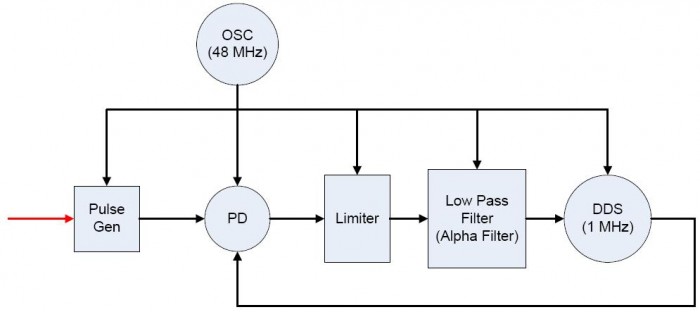
The diagram follows the form of the classic PLL with the exception of the limiter function following the phase detector PD. A single 48 MHz reference oscillator OSC provides the clock for all of the digital circuits which implement the DPLL described by the diagram.
The red external signal input is processed in the OSC clock domain to avoid meta-stability issues. The pulse generator is a simple function which provides a meta-stable immune pulse equivalent to the external 1PPS time reference to the DPLL's phase detector. Operating the DPLL in this manner avoids meta-stable events with respect to the 1PPS signal which can potentially result in missing one or more the external time reference pulses. Since the period of the external 1PPS signals is so long, missing any of them can have catastrophic results on the DPLL.
The phase detector PD measures the difference between the digital oscillator DDS and the external 1PPS signal. The referenced article on digital phase-locked techniques provides a discussion on one of the common approaches for measuring the phase error: a multiplier. The PD used in this application will not be a simple multiplier. Instead, this application will use a PD known as a Phase-Frequency Detector (PFD), which I will describe below.
The limiter simply prevents large initial phase errors from driving the digital oscillator too hard and extending the time needed to establish lock. The limiter restricts the rate of change that the DPLL can track, but in this particular application, the external signal is not variable: it has a fixed period of 1 second and does not vary in any substantial manner. Thus, the limiter actually speeds acquisition in this application by restricting the adjustment range of the digital oscillator's frequency due to large initial phase differences.
Following the limiter is the loop filter. This particular loop filter is designed so that no multipliers are needed in its implementation. It is an implementation of a standard filter known as an $\alpha$-filter where the coefficients are defined as negative powers of two:
$$ \alpha = {{1} \over {2^m}}. \tag {1} $$
The discrete $\alpha$-filter is defined as:
$$ y[n] = \alpha x[n]+(1-\alpha) y[n-1] = \alpha x[n] + y[n-1] - \alpha y[n-1] \tag {2} $$
Finally, the digital oscillator is implemented using a Direct Digital Synthesizer (DDS). Thus, in this application, the DDS is simply an accumulator (integrator) that adds the phase error output of the filter to itself. The rate at which the accumulator overflows represents the frequency of the digital oscillator. As implemented, the DDS will have an inherent jitter that is equal to the period of its reference oscillator: $ \frac{1}{48\text{MHz}} = 20.833\bar3 ns $.
Phase-Frequency Detector (PFD)
Instead of a multiplier, as described in the referenced article, the phase detector used in this application utilizes a PFD to measure the phase and frequency difference between the external timing reference and the DDS oscillator. A multiplier-based phase detector establishes a quadrature relationship between the external reference and the digital oscillator. In this application, the desired phase relationship between the external timing reference and the digital oscillator is 0 degrees rather than -90 degrees, i.e. quadrature. On the other hand, a PFD establishes a 0 degree relationship between the external timing reference and the digital oscillator, which is why it is used in this application.
A PFD works by using the timing relationship between the external and internal signals to increase and decrease the Frequency Control Word (FCW) used by the digital oscillator. In an analog implementation, fixed positive and negative current sources are used to tune the PLL oscillator, and when the signals are aligned, the current sources are disabled, i.e. tri-stated.
The digital PFD used in this application must emulate the behavior of its analog counterpart. That is, while the external and internal signals being compared are not aligned, the FCW presented to the digital oscillator changes in discrete steps which correspond to the current source strengths used in an analog PFD. When the signals are aligned, the FCW must maintain its value as it would with an analog PFD.
Assuming digital logic values for the external and internal signals, the operation of a digital PFD can be described mathematically by the following three equations:
$$ {FCW}[n] = \begin{cases} {FCW}[n-1] & \text{$S_X[n] = S_I[n]$} \\ {FCW}[n-1] + {FCW}_{ADJ_+} & \text{$S_X[n] > S_I[n]$} \\ {FCW}[n-1] + {FCW}_{ADJ_-} & \text{$S_X[n] < S_I[n]$} \end{cases} \tag {3} $$
The first case ensures that the FCW does not change when the phase/frequency difference is zero, the second case increases the frequency of the digital oscillator when the external timing signal leads the internal signal, and the third case decreases the frequency of the digital oscillator when the external timing signal lags the internal signal.
The values ${FCW}_{ADJ_+}$ and ${FCW}_{ADJ_-}$ are the discrete values needed to adjust the number of digital oscillator cycles by 1 over the period of the external timing signal, which in this application is 1 second. It turns out that these values can be easily calculated using the frequency of the external timing signal and the frequency of the digital oscillator's reference clock. In this application, therefore, these discrete adjustment values are computed using the following two equations:
$$ {FCW}_{ADJ_+}=\frac{f_{S_X}}{f_\text{Osc}}2^{32}=\frac{1\text{Hz}}{48\text{MHz}}2^{32}=89.478485\bar3=89 \tag {4} $$
$$ {FCW}_{ADJ_-}=-\frac{f_{S_X}}{f_\text{Osc}}2^{32}=-\frac{1\text{Hz}}{48\text{MHz}}2^{32}=-89.478485\bar3=-89 \tag {5} $$
The mechanism used in this application for determining the phase error is to represent the external timing signal, ${S_X}[n]$, and the internal timing signal, ${S_I}[n]$, as square waves using toggle flip-flops (FFs). The external timing signal pulse drives a toggle FF, and the overflow pulse from a counter driven by the digital oscillator similarly drives a toggle FF. (The counter overflows at the desired number of digital oscillator cycles per external timing signal period. In other words, in this application, the counter overflow value is equal to the nominal frequency of the digital oscillator.) These two signals, ${S_X}[n]$ and ${S_I}[n]$, are then evaluated using Eq 3 above to determine the FCW to be applied each clock cycle to the $\alpha$ filter and subsequently to the digital oscillator.
I added the limiter in this application to limit the amount of change applied to the FCW of the digital oscillator per period of the external timing signal. If the limiter activates, then the PFD holds the last value of the FCW until the next edge of either the external or internal timing signals. Limiting the rate of change of the digital oscillator's frequency has a tendency to slow the phase-lock process, However, in this application, limiting appears to improve the ability of the DPLL to lock over a wide range of initial conditions and avoiding saturation and/or roll-over of the digital oscillator's FCW, which is fatal to the operation of the DPLL.
Digital Oscillator
The digital oscillator is implemented as a DDS. The PFD provides a FCW which is integrated in an accumulator. The rate at which the accumulator overflows is equal to the frequency.
Like any other sample data system, the Nyquist Criterion applies. This means that the maximum frequency that can be produced is less than $\frac{1}{2}$ the frequency of the reference oscillator. Similarly, the maximum value of the FCW must be less than $\frac{1}{2}$ of the unsigned range of the digital oscillator's accumulator. In mathematical terms, the maximum frequency and the maximum FCW are defined by the following two equations:
$$ f_{\text{Max}} \lt \frac{f_{\text{Osc}}}{2} \tag {6} $$
$$ {FCW}_{\text{Max}} \le 2^{31}-1 \tag {7} $$
For completeness, the digital oscillator is implemented as an accumulator:
$$ DDS[n] = DDS[n-1] + FCW[n] \tag {8} $$
The nominal FCW, i.e. the initial condition of the PFD, is determined by the following equation:
$$ FCW_0 = \frac{f_{\text{DDS}}}{f_{\text{Osc}}}2^{32}=\frac{1\text{MHz}}{48\text{MHz}}2^{32}= 89478485.\bar3=89478485\tag {9} $$
Phase-Lock Detection
In this application, I implement phase-lock detection using a magnitude comparator and a re-triggerable counter. The magnitude comparator monitors the error count of the limiter. If the error count is less than a fixed threshold value, then the counter counts down. If the error count exceeds the threshold while the counter is counting down, then the counter is re-triggered.In the current application, the error counter is set to count 16 periods of the external timing reference signal. Thus, the error count must be below the threshold for 16 consecutive periods before phase-lock is declared. Given the general stability of the GPS 1PPS signal, setting the phase-lock indication threshold to 16 is a bit conservative.
Once the DPLL is locked, the DPLL provides the 1PPS timing signal to any devices which require it. If the error count increases above the threshold after phase-lock is achieved, the DPLL holds the digital oscillator at the last frequency, and supplies a stable clock and 1PPS reference. Tracking and re-locking to the external 1PPS timing signal will occur once the 1PPS signal is restored.
Reference Design
I've used the approach discussed above to create a number of DPLLs used for aligning a local oscillator to the 1PPS timing signal output of GPS receivers. The 1PPS-DPLL reference design provided at the link is a synthesizable Verilog project which can be used to maintain a precision clock and time reference during times when the 1PPS signal is lost by the GPS receiver.The Verilog testbench included demonstrates the operation of the 1PPS DPLL core. The digital oscillator initial condition was greatly disturbed specifically to demonstrate the digital oscillator slewing actions that the PFD generates as the DPLL is attempt lock to the 1PPS signal. The following diagram provides a graphical view of the DPLL in action trying locking to the external 1PPS signal, xPPS_In, under the adverse initial conditions.
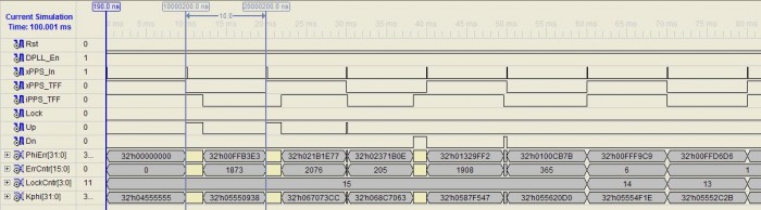
The toggle FF for the external timing signal, xPPS_TFF, is a nice square wave as expected. Since the initial condition of the digital oscillator places the initial frequency well below the desired 1 MHz nominal frequency, the width of the internal toggle FF is longer than the period of the external timing signal. This results in the PFD Up signal being asserted, and the FCW being increased. The initial increase in the FCW produces a decrease in the width of the iPPS_TFF signal, but that is not enough so it is followed by two additional increses in the FCW. The result is that the digital oscillator is now too fast, so decreases to the FCW follow. After two FCW decreases, i.e. Dn asserted, the two toggle FF signals are nearly perfectly aligned in frequency and phase. Thus, the lock detector counter begins its count down and when it reaches 0, the Lock signal will be asserted.
Conclusion
This article has presented an implementation of a DPLL that is able to lock to an external 1PPS timing signal. The article has also provided a link to the source of a synthesizable DPLL core. I welcome any constructive comments on the article and the reference design.
Correction
The logic required to coast and re-lock the DPLL following the loss the external timing reference has been corrected to behave as defined. The logic required to perform coast and re-lock after losing the external timing reference is different for a DPLL using the Phase-Frequency Detector. A prior implementation used a counter-based approach, and the coast and re-locking logic worked correctly for that phase detector. The coast and re-locking logic for that DPLL implementation was not changed when its phase detector was replaced by the PFD described in this article.
The following diagram shows the entire process, initial lock, loss of external timing reference, and re-locking when external timing reference restored:
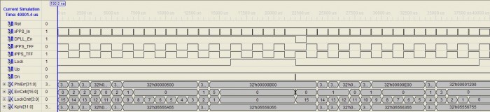
The new logic introduces no error in the digital oscillator's FCW when lock is lost due to the loss of the external timing signal. When the DPLL reacquires the restored external timing signal, there is also only a minor amount of error that must be driven out. (Note: this simulation was time scaled to 1000 Hz instead of 1 Hz.)
- Comments
- Write a Comment Select to add a comment

I enjoyed this article and am incorporating the design into an FPGA currently. Is there a contact email for the author? I have a few questions.
Best
Kevin.
Check the license headers of the source files.
Hello,
I am having difficulties in controlling duty cycle of output using this code. I have configured the code for generating 10MHz @ 50MHz. but i am getting variable duty cycle at NCO_Out. (i.e. 40% and 60% at different times). Can anyone please help me correcting that. any help will be appreciated. thanks in advance.
Ahsan:
The nature of the DPLL produces the nearest match to the configured operating frequency, while simultaneously locking to an external high precision signal such as the 1PPS signal output from an embedded GPS receiver. As you approach the Nyquist frequency of your oscillator (25MHz in your case), the NCO will produce the desired frequency (10MHz in your case) with greater variations in the duty cycle.
In this application, the oscillator (50MHz in your case) is not being adjusted in any way. Its frequency relative to the external reference is being measured, but its actual frequency / phase is not being physically changed. Therefore, the circuit will always produce an output with some period errors. On average, the period and frequency of the "programmed" output frequency of the circuit will be the desired value and in phase relative to the external reference signal, i.e., 1PPS from GPS.
The purpose of the circuit was measure the frequency of the oscillator, relative to the external input, by adjusting the frequency control word of the NCO / DDS. In this manner, if the external input signal is lost, the DPLL circuit can maintain time with a drift characteristic that is much improved from the basic drift characteristic of the reference oscillator. In this way, low cost standard crystal oscillators with frequency accuracies of +/-50ppm to +/-150ppm could be used to maintain time for several minutes / hours to GPS-like accuracy without a GPS 1PPS input.
If you require a 10MHz time stamp frequency with less period jitter, I would suggest that you need to increase the frequency of your base oscillator, i.e., increase the frequency of your 50MHz oscillator. The issue you will have, especially if you implement the DPLL in an FPGA as I did, is that the higher operating frequency of your reference oscillator will require greater performance from the NCO / DDS component.
There's always a trade off between simplicity and accuracy. If you absolutely need accuracy, then there's no escaping the need to form a true PLL using a temperature-stabilized, voltage-controlled, adjustable crystal oscillator. Unfortunately, in the application for which I developed the 1PPS DPLL described in this article, that complexity was not an option since the design was already complete before the requirement to coast through a GPS signal fade was levied on the design.
Goodmorning, nice article.
I am newbie about verilog and I am trying to create a sync module as basetime for seismic instrument.
I need to create a 1.024 MHz clock from 1 Hz PPS (provided by GPS module).
Due I am a beginner in verilog, is there a way to get support understanding behaviour of above modules withoud bothering the author? Thanks.
To post reply to a comment, click on the 'reply' button attached to each comment. To post a new comment (not a reply to a comment) check out the 'Write a Comment' tab at the top of the comments.
Please login (on the right) if you already have an account on this platform.
Otherwise, please use this form to register (free) an join one of the largest online community for Electrical/Embedded/DSP/FPGA/ML engineers:


