


Feedback Controllers - Making Hardware with Firmware. Part 9. Closing the low-latency loop
It's time to put together the DSP and feedback control sciences, the evaluation electronics, the Intel Cyclone floating-point FPGA algorithms and the built-in control loop test-bed and evaluate some example designs. We will be counting the nanoseconds and looking for textbook performance in the creation of emulated hardware circuits. Along the way, there is a printed circuit board (PCB) issue to solve using DSP.
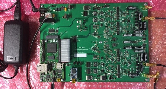
Fig 1. The evaluation platform
Additional design notes will be published in due course, on the project website here and the latest developments can be followed on Twitter @precisiondsp. and LinkedIn
- Part 9: Closing the low-latency loop (this part)
- Part 8: Control Loop Test-Bed
- Part 7: Turbo-charged Oscillators
- Part 6: Self-Calibration, Measurements and Signalling
- Part 5: Some FPGA Aspects
- Part 4: Engineering of Evaluation Hardware
- Part 3: Sampled Data Aspects
- Part 2: Ideal Model Examples
- Part 1: Introduction
As ever, it should be noted that any examples shown may not necessarily be the best or most complete solution.
Contents of this Article
- Project Recap and Context for this article
a. The requirement for high-performance low-latency controllers - Parameters for the design examples
a. ADC, DAC and DSP Sample rates
b. Digital controller type - Measurements
a. MATLAB reference measurements
b. Test configurations
c. Test signals
d. Design evaluation measurements - Example designs and results
a. Tests on a short circuit
b. A Controller
c. Circuit1
d. Circuit2 + a hardware problem and a solution using DSP
e. Circuit3 - Discussion and Conclusions
1. Project Recap and Context for this article
This project is concerned with the development of high-speed low-latency controllers and an example closed-loop application that can make arbitrary (within reason) 1 and 2 port electrical/electronic circuits.
In Part 1 we asked a simple question :-
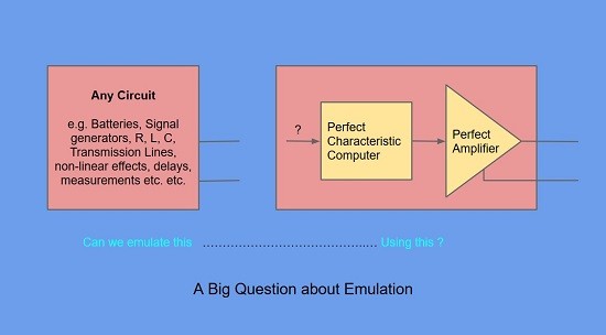
Fig 2. A simple question
and answered with a simple example :-
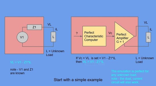
Fig 3. A simple example showing how we can emulate hardware by computing circuit characteristics.
An evaluation unit has been designed and manufactured to evaluate what levels of functionality and performance can be achieved using modestly-priced and readily available technology with a particular emphasis on floating-point FPGA devices such as the Cyclone V and the emerging Cyclone 10 GX parts from Intel.In previous articles 1 to 8, we have considered the basic principles of circuit emulation, the engineering of technology evaluation hardware, some characteristics and challenges for sampled data feedback controllers and provision of built-in test and measurement facilities.
Our question in Fig 2. is now updated for the real world.
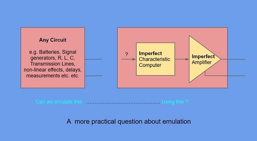
Fig 4. Engineers have to provide solutions with non-ideal components
These first designs will be simple in that the loop controller DSP will be just a single Biquad IIR Filter. Also, it will run at a lower sample rate (DSP rate = 1.6Msps) than future examples.
We will also look at an issue due to higher than wanted printed circuit board (PCB) capacitance and see how it can be solved with the aid of DSP and a PCB re-spin avoided.
a. The requirement for high-performance low-latency controllers
Closed-loop applications in general, typically require low-latency controllers, to avoid a reduction of stability margins and other undesirable response characteristics.
In addition, the circuit emulator application requires not just a stable response that converges to a desired value, but a response that is accurate at every instant in time.
Our controllers must therefore provide not just stability and eventual convergence, but they must result in a loop with faithful characteristics at all times.
2. Parameters for the design examples
a. ADC, DAC, DSP Sample rates
ADC Sample Rate -The 16 bit ADC sample rate is set to 8Msps (Max = 15Msps)
DAC Sample Rate -The 16 bit DAC sample rate is set to 24Msps (Max = 48Msps)
DSP Sample Rate - The floating-point Biquad IIR filter is designed for a sample rate = 1.6Msps. The Maximum is yet to be determined but may be 8Msps for the Cyclone V and higher for the Cyclone 10 GX.
b. Digital controller type
The loop controller is based on a single floating-point Biquad IIR of type II transposed form as shown below.
![]()
Fig 5 A Biquad of type II Transposed form shown using MATLAB/Simulink block conventions
Note - Other sources may use different gain lettering and/or alternative gain/summer sign convention.
3. Measurements
a. MATLAB reference measurements
For each Controller or Circuit characteristic to be evaluated, a MATLAB model of the characteristic equations is generated and the results exported to a .csv file for import and display along side the practical measurements. There are two types of measurements :-
- Controller applications - This is a (voltage in)/(voltage out) measurement and the results are presented as Gain(dB), Phase (degrees) and Latency(ns) where Latency is defined as (Phase/360) / frequency , for each frequency reported.
- Circuit/Port applications - This is a voltage/current measurement and the results are presented as Impedance Magnitude(ohms), Impedance Phase (degrees) and Latency(ns) where Latency is defined as before.
b. Test configurations
These are covered in some detail in Part 8 of this series and look like this :-
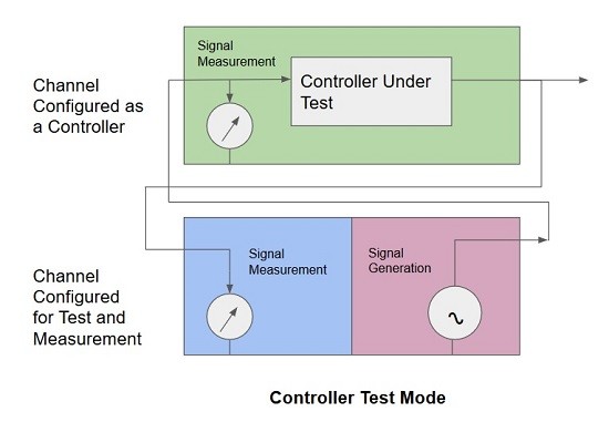
Fig 6. Test Configuration for Controller applications
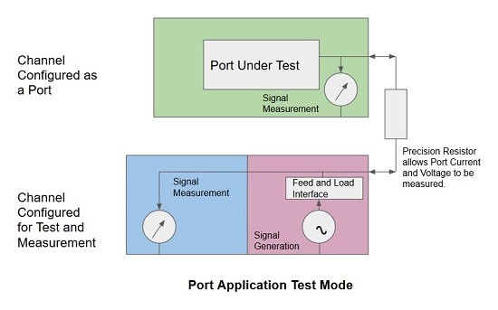
Fig 7. Test Configuration for Circuit/Port applications
c. Test signals
The test signal is an IFFT based method which is again described in Part 8 of this series and consists of a large number of sine waves generated simultaneously to allow a chosen band of frequencies to be analyzed from a dual-channel time record of 2 x 32768 samples at a rate of 8Msps i.e. a total measurement time of only 4.096ms for 2 channels captured simultaneously.
Here is a sample of the test signal used in for the evaluations in this article.
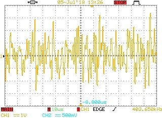
Fig 8. Oscilloscope trace of an IFFT based test signal section
d. Design evaluation measurements
Referring to Figs 6 & 7 above, there are 2 sets of voltage measurements collected simultaneously by the ADCs situated in each channel. This allows either the Controller input voltage and output voltage time records or the Circuit/Port voltage and current time records to be collected.
Once we have waited 4.096ms for the records to be collected, we can perform non-windowed FFTs on them to produce traditional gain/phase or impedance magnitude/phase plots along with other interpretations such as latency and in the future, Return Loss for example.
Our practical results will be plotted graphically along with the MATLAB reference curves, to allow comparison and assessment.
4. Example designs and results
The design examples will start with a system test to create a basic confidence in the measurement system.
After the test case, 1 controller example and 3 Circuit/Port examples will be evaluated. These will be formulated as both Circuit Models and MATLAB Models and MATLAB reference results will be generated. The appropriate controller IIR/Biquad characteristics will then be calculated and passed to the FPGA floating-point maths blocks and associated trim settings.
The Controller transfer function and Circuit/Port Impedance characteristics will then be measured using the IFFT based signal and the results plotted along with the MATLAB reference curves.
The actual design characteristics are chosen purely to illustrate an interesting range of responses and may or may not have any practical application use.
Small steps for the 1st results (More speed and complexity later)
- These are lower DSP sample-rate examples (1.6Msps) to get some initial performance results.
- The Digital Filter is a single floating-point Biquad, so only simple circuits can be constructed for these first tests.
a. Tests on a short circuit
Test Description - Both Channels fed with the same test signal.
Setup - This test applies the IFFT test signal to both Channel measurement i/ps via 15.2cm cables.
Expectation - The expectation is to see very little Magnitude, Phase and Latency (as defined above) difference between the 2 Channel signals.
Circuit Model - Its equivalent to a short circuit
MATLAB Model - None
Results
Fig 9a. Magnitude difference between the 2 measurement channels fed by the same test signal
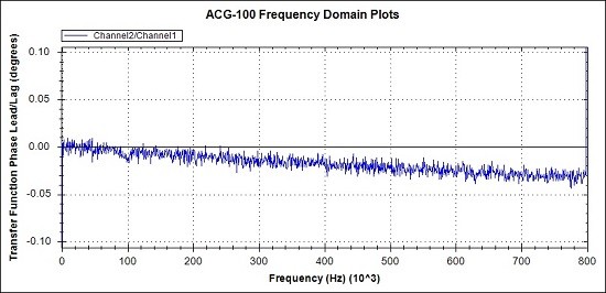
Fig 9b. Phase difference between the 2 measurement channels fed by the same test signal
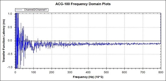
Fig 9c. Latency difference between the 2 measurement channels fed by the same test signal
Comments
Magnitude matching on a smoothed response is better than 0.01dB.
Phase matching is better than 0.05 degrees.
The Latency matching plot data is ill-conditioned for low frequencies where 1/f is relatively large. It is better to look at Phase for low-frequency assessment. At other points the Latency matching is around 200ps on average.
In the context of this project these levels of matching are fine. There is no point is calibrating these tiny mismatches out.
b. A Controller
Test Description - An example Controller is implemented for Transfer Function accuracy evaluation.
Setup - This test applies the IFFT test signal to input port of Channel 2 (the controller). Measurements are made on Channel 2 input and output ports and the transfer function is calculated.
Expectation - Close correspondence between measured results and MATLAB reference figures.
Circuit Model - Could be made, but MATLAB transfer function is more appropriate.
MATLAB Model - The MATLAB Laplace transfer function for this example is :-
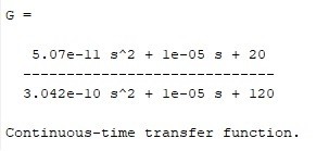
Fig 10. Transfer Function of the Example Controller
Results
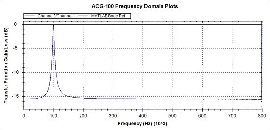
Fig 11a. Overview of Magnitude response. MATLAB reference (Magenta), Measurements (Blue)
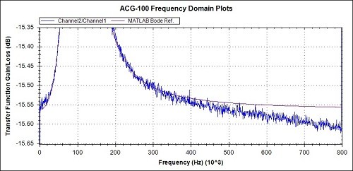
Fig 11b. Magnitude detail from Fig 11a
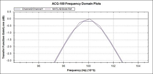
Fig 11c. Magnitude detail from Fig 11a
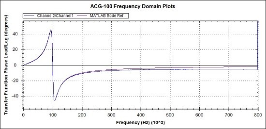
Fig 12a. Overview of Phase response. MATLAB reference (Magenta), Measurements (Blue)
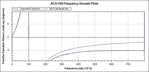
Fig 12b. Phase detail from Fig 12a
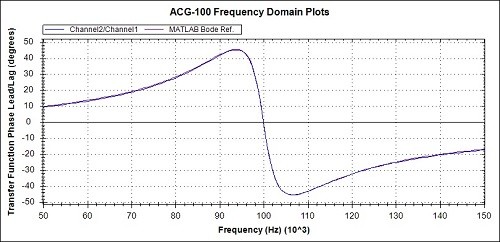
Fig 12c. Phase detail from Fig 12a
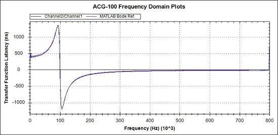
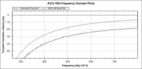
Fig 13b. Latency detail from Fig 13a
In general, looking at the 3 overview graphs of Figs 11a, 12a and 13a the correspondence between the practical measurements and the MATLAB reference graphs is very promising.
Observations of the measured values compared to the MATLAB references, from the detail graphs are :-
- The Magnitude peak and Phase zero crossing at 100kHz are accurately positioned
- The Magnitude values around the peak, average at around 0.1dB low
- The Magnitude is around 0.05 dB low at 800kHz
- The Phase is around 3 degrees lagging at 800kHz
- The Latency is around 10ns over at 800kHz
The causes of these inaccuracies and the corrections to be applied will be discussed when all the example results have been presented.
c. Circuit 1
Test Description - An example Circuit is implemented for Impedance accuracy evaluation.
Setup - This test applies the IFFT test signal to the Circuit port of Channel 2 . Measurements are made on the Channel 2 port and a current-sense resistor. The Circuit port impedance is then calculated.
Expectation - Close correspondence between measured results and MATLAB reference figures.
Circuit Model - This circuit has an impedance of 100 ohms at low and high frequencies and a peak of 1000 ohms at 100kHz.
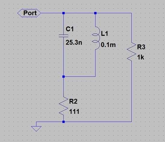
Fig 14. An example circuit to be emulated.
MATLAB Model - The MATLAB code for this circuit is:-
opts = bodeoptions('cstprefs');
opts.FreqUnits = 'Hz';          % change the bode options to Hz

s = tf('s');       % declare the s operator
% This is an example of a Port impedance of 100 ohms with a peak of
% 1k ohms at 100kHz
% The circuit is 1000 ohms in // with (111 ohms + (25.3nF//0.1mH))
%
Rs1 = 111;
Rp1 = 1000;
L = 1e-4*s;
C = 1/(25.3e-9*s);
ParaLC = 1/((1/L) + (1/C));
B1 = Rs1 + ParaLC;
PortZ = 1/( (1/Rp1)+(1/B1) );

figure(1)
bodeplot(PortZ,{1,100000000},opts);  % show Port Z
grid on  % grid on
Fig 15. MATLAB Code for the example Circuit
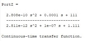
Fig 16. The transfer function of the circuit impedance
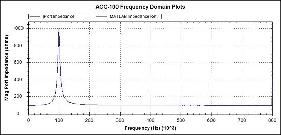
Fig 17a. Overview of Magnitude response. MATLAB reference (Magenta), Measurements (Blue)
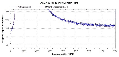
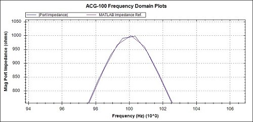
Fig 17c. Magnitude detail from Fig 17a
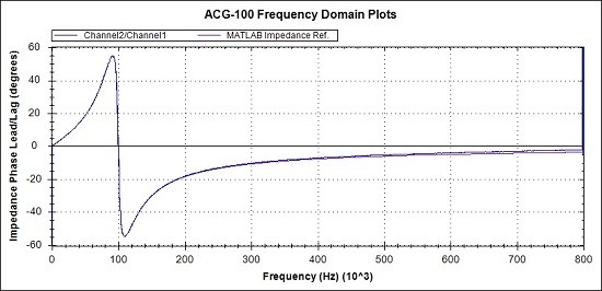
Fig 18a. Overview of Phase response. MATLAB reference (Magenta), Measurements (Blue)
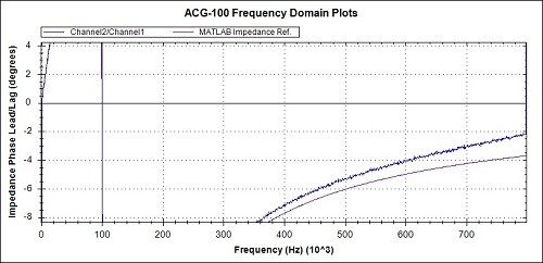
Fig 18b. Phase detail from Fig 18a
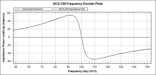
Fig 18c. Phase detail from Fig 18a
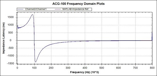
Fig 19a Overview of Latency response. MATLAB reference (Magenta), Measurements (Blue)
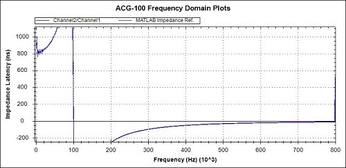
Fig 19b. Latency detail from Fig 19a
Comments
The 3 overview graphs of Figs 17a, 18a and 19a show a high degree of correspondence between the practical measurements and the MATLAB reference graphs.
Observations of the measured values compared to the MATLAB references, from the detail graphs are :-
- The phase at 800kHz is around 2 degrees advanced representing a 5ns advance in latency.
As before, the causes of inaccuracies and the corrections to be applied will be discussed when all the example results have been presented.
d. Circuit 2 + a hardware problem a solution using DSP
Test Description - An example Circuit is implemented for Impedance accuracy evaluation.
Setup - This test applies the IFFT test signal to the Circuit port of Channel 2 . Measurements are made on the Channel 2 port and a current-sense resistor. The Circuit port impedance is then calculated.
Expectation
- Close correspondence between measured results and 500 ohms
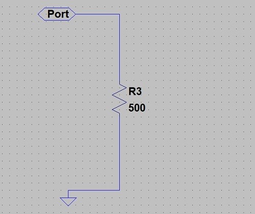
Fig 20. A very simple 500 ohm resistor circuit
Results
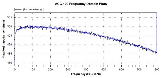
Fig 21. Detail of Magnitude response. Measurements (Blue)
Fig 22. Detail of Phase response. Measurements (Blue)
Comments
We don't need MATLAB reference graphs because we are simply expecting 500 ohms and 0 degrees phase.
The two obvious unwanted effects we can see are :-
- A low frequency droop of around 4 ohms at low frequencies
- A progressive high frequency droop of around 15 ohms at high frequencies
- A corresponding progressive phase lag of around 14 degrees at high frequencies
Similar investigations indicate that the cause of the high frequency magnitude droop and phase lag, is capacitance associated with the port access circuitry. Although care was taken in the design and layout, it looks like we could benefit from a revised arrangement.
Note - The parasitic capacitance issue does not significantly affect Controller applications, as a) the access arrangements are simpler and b) Low impedance drives to the input and low impedance outputs are used.
But, let's see what can be done using the unit phase compensator and our single Biquad controller to account for the estimated 100pF of parasitic capacitance.
Results with simple compensation for parasitic capacitance
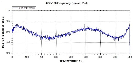
Fig 23. Detail of Magnitude response. Measurements (Blue)
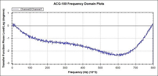
Fig 24. Detail of Phase response. Measurements (Blue)
With a small amount of design effort we have reduced the maximum magnitude error from around 15 ohms to around 3 ohms or 0.6%.
The maximum phase error is reduced from 15 degrees to 2.4 degrees.
It is anticipated that an additional Biquad filter stage will result in further improvements.
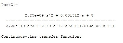
e. Circuit 3
Test Description - An example Circuit is implemented for Impedance accuracy evaluation.
Setup - This test applies the IFFT test signal to the Circuit port of Channel 2 . Measurements are made on the Channel 2 port and a current-sense resistor. The Circuit port impedance is then calculated.
Expectation - Close correspondence between measured results and MATLAB reference figures.
Circuit Model - This circuit has an impedance of close to 8 ohms at low frequencies and a rising then falling characteristic at higher frequencies. It also includes a capacitor representing PCB and access circuit capacitance.
MATLAB Model - The MATLAB code for this circuit is :-
opts = bodeoptions('cstprefs');
opts.FreqUnits = 'Hz';          % change the bode options to Hz

s = tf('s');       % declare the s operator

% The circuits is 1.5mH + 8 // with 1.5nF + 1000
%
R1 = 8;
R2 = 1000;
L = 1.5e-3*s;
C = 1/(1.5e-9*s);
B1 = R1 + L;
B2 = R2 + C;
Cpara = 1/(100e-12*s);% PCB capacitance

PortZ = 1/( (1/B1)+(1/B2)+(1/Cpara) );

figure(1)
bodeplot(PortZ,{1,100000000},opts);  % show Port Z
grid on  % grid on
Fig 26. MATLAB Code for the example Circuit
Results
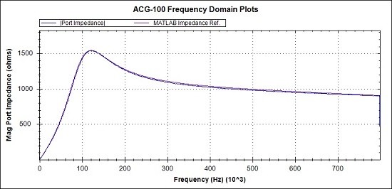
Fig 28. Overview of Magnitude response. MATLAB reference (Magenta), Measurements (Blue)
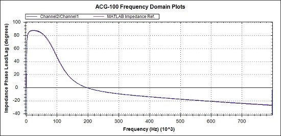
Fig 29. Overview of Phase response. MATLAB reference (Magenta), Measurements (Blue)
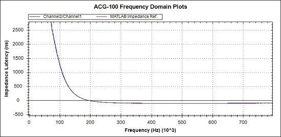
Fig 30. Detail of Latency response. MATLAB reference (Magenta), Measurements (Blue)
Comments
In the general views of Figs 28 and 29 and the detail view of Fig 30, the measured responses are seen to be virtually coincident with the MATLAB reference figures.
There is little value in looking at the fine detail as the aim will be to use the previously proven Biquad to counter the parasitic capacitance and then add another Biquad to produce the Inductor, Capacitor and two resistors that we actually want.
As we are limited to just one Biquad at present, the full analysis will wait until next time.
5. Discussion and Conclusions
This has been a first look at the initial performance results for the low-latency controller and the closed-loop arbitrary circuit emulator.
This exercise was set at a low DSP sampling rate of 1.6Msps although measurements are made at 8Msps. Later we anticipate increasing the DSP sampling rate to match the measurement rate at 8Msps.
Also, we limited the number of Biquad filter stages to just 1. In theory there are enough DSP resources in the Intel Cyclone V for another 40 Biquads on each channel.
Controller and Circuit emulation examples were developed to exhibit sharp characteristics, flat characteristics and in one example a circuit impedance range from 8 ohms to > 1.5k ohms.
There was an initial disappointment that the Port access circuits exhibited a higher parasitic capacitance than wanted, at around 100pF, but it turned out that this could be effectively cancelled out by use of the existing phase compensation circuit along with suitable Biquad settings. Long term, this parasitic capacitance can be reduced with some component changes and additional PCB trace voiding, but for now it is fine to free up 1 Biquad to make the fix.
There are a few non-ideal elements that have been identified, that affect the performance. These are :-
- Port access circuit parasitic performance - fixed by DSP and phase correction circuit
- Suspected Port amplifier device low frequency droop - will be easily fixed by DSP
- DAC reconstruction - Zero order hold amplitude loss - will be easily fixed by DSP
The measurement system, which basically comes for free as part of the controller DSP is a joy to work with and provides a sophisticated wide-band time domain and frequency domain analysis from a 4.096 ms data capture. I was not expecting to have a clear view down to sub degree, sub ns and mdB levels, but the results do indeed allow inspection at these levels.
These first results from the examples, provide great encouragement for the next phase of faster, more complex circuits. Whilst there are some residual small unwanted effects still to be resolved, many of the practical results are close enough to the MATLAB theoretic plots that there is no pressing need to look for further improvement.
Conclusions
A demonstration of low-latency controllers and closed-loop applications that make use of them has been demonstrated.
The technology evaluation system has proven capable of performing well on an initial set of exercises.
A notional objective to provide a 10 x Speed and 10 x Complexity over a previous historical design now looks achievable and the opportunities are even greater if a move is made from the Cyclone V FPGA to the Cyclone 10 GX FPGA.
All is set fair with the existing hardware for the next set of tests at a higher DSP sampling rate and more controller Biquads.
Thank you for your interest, Steve Twitter @precisiondsp. and LinkedIn
- Comments
- Write a Comment Select to add a comment
To post reply to a comment, click on the 'reply' button attached to each comment. To post a new comment (not a reply to a comment) check out the 'Write a Comment' tab at the top of the comments.
Please login (on the right) if you already have an account on this platform.
Otherwise, please use this form to register (free) an join one of the largest online community for Electrical/Embedded/DSP/FPGA/ML engineers:


